Understanding SMT Printed Circuit Boards in Modern Electronics

Key Takeaways
SMT (Surface Mount Technology) printed circuit boards (PCBs) have transformed the landscape of electronics through their unique features and benefits. At the core of pcb assembly is the process where electronic components are mounted directly onto the surface of a PCB, allowing for more compact designs and improved functionality. One significant advantage of SMT technology is the reduction in the overall size of electronic devices, facilitating advancements in miniaturization. This has enabled manufacturers to create smaller, more powerful devices that cater to modern consumer demands for portability and efficiency.
Moreover, pcba processes enhance production efficiency and reduce assembly times compared to traditional methods. The integration of automated assembly lines in SMT manufacturing has led to higher precision and lower production costs, which can be particularly beneficial for companies seeking to innovate quickly while managing expenses effectively.
“Leveraging SMT technology not only boosts productivity but also positions companies at the forefront of technological advancements in electronics.”
As technology progresses, it’s crucial for businesses involved in electronics manufacturing to adopt SMT PCBs in their operations. This move ensures they remain competitive and responsive to market trends. Understanding these key aspects will enable stakeholders to appreciate the pivotal role that SMT printed circuit boards play in shaping modern electronics while continually pushing the boundaries of device performance.
Introduction to SMT Printed Circuit Boards
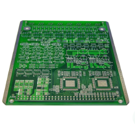
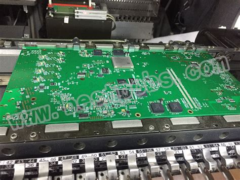
Surface Mount Technology (SMT) has revolutionized the landscape of pcb assembly, becoming an essential aspect of modern electronics. SMT printed circuit boards (PCBs) feature components that are directly mounted onto the surface of the board, which contrasts with traditional through-hole technology where components are inserted into drilled holes. This innovative approach allows for a more compact design, drastically reducing the size and weight of electronic devices. The adoption of SMT has enabled manufacturers to create high-density assemblies and achieve substantial improvements in performance and reliability.
The advantages associated with using SMT PCBs are numerous and far-reaching, including improved electrical performance due to shorter connections and reduced parasitic inductance. Furthermore, the automated pcba process enhances production efficiency and lowers manufacturing costs. As consumer demand for smaller, more advanced devices grows, the role of SMT continues to expand, paving the way for further innovations in miniaturization and device capabilities. Manufacturers are increasingly recognizing that SMT is not just a method; it is a critical strategy for staying competitive in the fast-evolving tech industry.
The Manufacturing Process of SMT PCBs
The manufacturing process of SMT printed circuit boards (PCBs) is a crucial aspect of modern electronics, fundamentally altering how devices are assembled and their overall performance. The process begins with the design and layout of the circuit board, which is usually created using specialized software. This design is then transferred to a photomask, which aids in the precise application of the conductive pathways that will eventually form the printed circuit. Once the layout is ready, a thin layer of copper is laminated onto a substrate material. Subsequently, a chemical process etches away unwanted copper, leaving behind the desired circuitry.
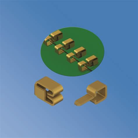
After this initial stage, solder paste—a mixture of small metal balls and flux—is applied to specific areas where components will be placed. This step is vital for achieving reliable pcb assembly as it facilitates the connection between components and the board. Next comes pick-and-place, where automated machines place surface-mount components onto the board with remarkable accuracy.
Once all components are in position, the assembly undergoes reflow soldering. This involves heating the entire board to melt the solder paste, effectively securing each component in place as it solidifies upon cooling. The significance of this process lies in its ability to support high-density boards that are critical for miniaturized devices.
Finally, after completing these stages, each pcba (printed circuit board assembly) is thoroughly tested for functionality and quality assurance before being packaged for shipment. The intricacies involved in this carefully orchestrated operation not only ensure performance consistency but also contribute significantly to innovations in device miniaturization and efficiency across various sectors within technology.
Advantages of Using SMT Technology
Surface Mount Technology (SMT) has revolutionized the way printed circuit boards (PCBs) are designed and assembled. One of the key advantages of SMT is its ability to enhance electrical performance while minimizing the physical footprint of electronic devices. This technology allows for the placement of components directly onto the surface of a PCB, eliminating the need for drilled holes and thereby reducing manufacturing complexity. As a result, PCB assembly (PCBA) becomes not only more efficient but also supports higher component density.
Furthermore, the use of SMT enables faster production rates due to automated assembly processes, significantly shortening time-to-market for new products. In modern electronics where performance is paramount, solder joint reliability is heightened with SMT due to better thermal and electrical characteristics. The capability to utilize smaller components means that devices can be more compact, contributing significantly to miniaturization trends in electronics. Ultimately, companies that adopt SMT technology can achieve greater flexibility in design and manufacturing processes while delivering devices with superior functionality and reduced costs, translating into immense value in today’s competitive landscape.
Impact of SMT PCBs on Device Performance
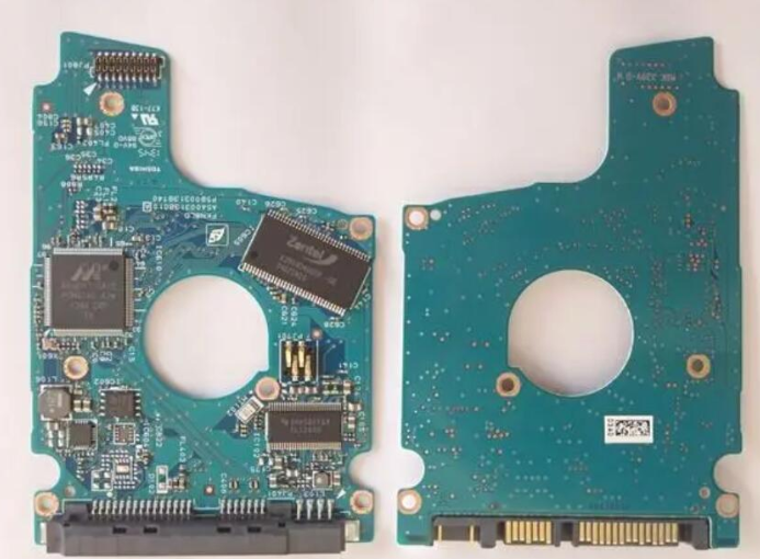
The emergence of SMT (Surface Mount Technology) in printed circuit board (PCB) design has significantly transformed device performance across various electronic applications. By facilitating a more compact design, SMT PCBs enable components to be placed directly onto the surface of the board, which reduces the overall footprint and enhances functionality. This is particularly crucial in modern devices that demand miniaturization without sacrificing performance. The process involved in pcb assembly allows for higher component density, leading to an increase in the number of functionalities within a smaller enclosure. As a result, devices can operate more efficiently with reduced signal pathways, which minimizes signal loss and enhances reliability. Furthermore, the efficiency of pcba processes has led to faster production cycles and improved quality control, contributing to better end-user experiences. The ability to integrate complex circuits into smaller spaces has not only optimized device performance but also opened pathways for innovations in design and technology across industries. In essence, the impact of SMT PCBs on device performance is profound, driving advancements that cater to consumer demands for smaller, faster, and more efficient electronics.
Miniaturization in Electronics: A Case for SMT
The integration of Surface Mount Technology (SMT) into the design and production of electronic components has been a game-changer for the tech industry, particularly in relation to miniaturization. As devices become increasingly compact and lightweight, the significance of SMT printed circuit boards (PCBs) cannot be overstated. This technology allows for a more efficient pcb assembly process by enabling components to be mounted directly onto the surface of a PCB rather than through holes, which was common in earlier technologies. The result is a remarkable reduction in the size of printed circuit boards, facilitating a higher density of components. As electronic devices continue to evolve, manufacturers can now fit more complex functionalities into smaller form factors, which is essential for mobile devices, wearables, and other portable technology. Furthermore, the use of SMT contributes to improved electrical performance and reliability due to shorter signal paths and reduced parasitic capacitance. The implications for product innovation are far-reaching; compact designs not only enhance user experience but also meet modern aesthetic standards that favor sleekness and portability. The continuous advancements in SMT technology are thus pivotal in driving forward the industry’s capability to deliver high-performance, miniaturized electronic solutions while maintaining cost-effectiveness during pcba processes.
Future Trends in SMT PCB Technology
As technology continues to advance, the future of SMT printed circuit boards (PCBs) appears increasingly promising. The integration of IoT (Internet of Things) devices has catalyzed a surge in demand for more compact and efficient pcb assembly processes. This trend necessitates innovations in design and materials, with a particular focus on flexible PCBs, which can host advanced functionalities while bending into intricate shapes. Moreover, 3D printing technology is making strides in PCB production, allowing for the rapid prototyping and manufacturing of custom designs that were previously unachievable. As we move forward, the incorporation of AI-driven design tools is expected to enhance design accuracy, streamline the pcba process, and reduce production costs. Additionally, sustainability is becoming a priority; manufacturers are exploring eco-friendly materials and processes to minimize waste during assembly, thus addressing environmental concerns while ensuring high performance. Overall, these trends signify a shift toward more innovative, efficient, and eco-conscious practices in SMT PCB technology.
Challenges and Solutions in SMT PCB Production
The production of SMT printed circuit boards (PCBs) comes with a unique set of challenges that manufacturers must navigate to ensure high-quality output. One significant challenge is achieving alignment accuracy during the pcb assembly process. Misalignment can lead to soldering defects, which may compromise the reliability of the final product. To combat this, advanced pcba technologies utilize precise pick-and-place machines that are equipped with sophisticated vision systems to ensure component placement is exact and consistent.
Another challenge lies in the management of thermal profiles during soldering. Excessive heat can damage sensitive components, while inadequate heat may result in insufficient soldering. Developing an optimal thermal profile requires meticulous calibration and testing, which can be resource-intensive. Manufacturers are increasingly turning to real-time monitoring systems that provide feedback during the soldering process, allowing for immediate adjustments that enhance integrity.
Furthermore, the miniaturization of components means that manufacturers must tackle issues related to component handling and integration. Smaller parts are often more prone to damage and require specialized equipment for handling. Solutions such as tailored workflow designs and customized tooling have emerged to address these complexities, ensuring parts are managed delicately without sacrificing throughput.
In summary, while challenges in SMT PCB production exist, innovative solutions such as automated systems for alignment, real-time thermal monitoring, and specialized handling equipment continue to advance the industry’s capability to meet demand for high-performance electronics.
Conclusion
In the realm of modern electronics, SMT printed circuit boards (PCBs) have become indispensable due to their numerous advantages and significant contributions to device performance. The evolution towards Surface Mount Technology (SMT) has facilitated the production of pcba, enabling the creation of more compact and efficient electronic devices. As technology continues to advance, the need for high-density interconnection and miniaturization is paramount, and SMT provides unparalleled solutions in meeting these demands. The dynamic nature of today’s electronics market necessitates that manufacturers adapt to new challenges while also embracing innovative pcb assembly methods. By utilizing SMT processes, companies can enhance manufacturing efficiency and achieve higher quality standards, which ultimately leads to improved reliability for end-users. As we look ahead, it is clear that SMT PCBs will play a crucial role in shaping the future landscape of electronics, driving innovation and efficiency in ways we are only beginning to explore.
FAQs
What is SMT assembly?
SMT assembly refers to the process of placing surface-mounted devices on a printed circuit board (PCB). This technology is pivotal in reducing the size and improving performance in modern electronics.
What are the benefits of SMT PCBA?
The benefits of SMT PCB assembly (PCBA) include increased component density, better performance, and enhanced reliability. It allows for more compact designs, which is crucial for today’s miniaturized devices.
How does SMT technology impact device performance?
SMT technology enhances device performance by providing shorter electrical paths, reducing signal loss and improving overall functionality. This results in faster operation speeds and greater efficiency.
Why is miniaturization important in electronics?
Miniaturization allows for smaller, more portable devices without sacrificing functionality. As electronic products become smaller, SMT PCBs enable manufacturers to create compact designs that are more versatile and user-friendly.
What challenges are associated with SMT PCB production?
Challenges include managing heat during production, ensuring accurate placement of components, and maintaining quality control during the PCB assembly process. Solutions often involve advanced technology like automated inspection systems.