Unleashing Innovation: The Evolution of Electronic PCBs in Modern Technology
Key Takeaways
Understanding the evolution and impact of printed circuit boards (PCBs) is crucial for anyone interested in modern technology. In the realm of pcb manufacturing, knowing the various processes involved is essential, as these determine the quality and performance you can expect from your electronic devices. You’ll find that pcb manufacturing companies are continuously innovating, which helps to optimize not only production efficiency but also to minimize pcb manufacturing costs. Innovations in technologies, such as advanced materials and automated fabrication techniques, have drastically improved the reliability and speed of PCBs, essential for high-speed data communication systems. The pcb manufacturing business has shifted toward designing high-density interconnect systems that offer compact solutions without compromising on performance. By grasping these key takeaways, you can better appreciate how innovations in PCB design and production directly influence various applications across multiple industries, ensuring a future where electronic PCBs remain at the forefront of technological advancement.
The Historical Context of Printed Circuit Boards
The history of printed circuit boards (PCBs) is a fascinating journey that reflects the rapid advancements in electronic technology. Your understanding of PCB manufacturing begins with the early days of electronics, where wires were painstakingly connected by hand. The evolution from this rudimentary wiring to printed circuit boards in the mid-20th century marked a pivotal moment in the electronics industry. It was during this era that PCB manufacturing processes were refined, allowing for more compact and reliable circuit designs. You’ll find that many modern pcb manufacturing companies can trace their roots back to this transformational period, as the demand for more efficient electronic devices increased.
As PCBs became integral to various applications, manufacturers had to address rising challenges such as miniaturization and complexity. This led to the development of advanced techniques and materials that reduced pcb manufacturing costs while enhancing performance. The introduction of multi-layered designs and high-density interconnects shaped how electronic devices are constructed today. By understanding this historical context, you can appreciate how PCB manufacturing business practices have evolved to meet the demands of modern technology and how they continue to play a crucial role in shaping innovations across numerous industries. For more on this topic, visit Andwin PCB.
Key Manufacturing Processes in PCB Production
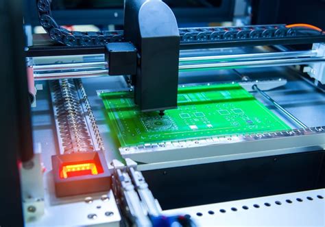
The journey of pcb manufacturing is intricate, involving several key processes that ensure the creation of reliable and high-performance printed circuit boards. To begin with, the process starts with design—this is where engineers utilize specialized software to create intricate layouts that dictate how components will be arranged and connected on the board. Following this stage, the fabrication process comes into play, where raw materials such as copper clad laminates are transformed through a series of steps including etching and drilling to create the desired circuitry paths.
Once fabricated, assembly is the next pivotal phase in the pcb manufacturing business, where various electronic components are meticulously placed onto the board. This may involve techniques like surface mount technology (SMT) or through-hole technology (THT), which contribute to different aspects of performance and cost-effectiveness. It’s essential to consider that while some PCB manufacturing companies might focus on low-cost alternatives, others vouch for premium materials and processes that enhance durability and functionality—this is reflected in different pcb manufacturing costs.
“Streamlining your processes by investing in quality materials can lead to long-term savings and better performance.”
As you navigate through these manufacturing stages, understanding each component’s role will empower you to appreciate how they collectively bring your electronic designs to life. The synergy between different processes ultimately leads to innovative solutions that can meet today’s demanding technological standards—highlighting why investing in professional pcb manufacturing is critical for future success.
Design Methodologies for Modern PCBs
The design methodologies for modern PCBs have evolved significantly, adapting to the demands of advanced electronics. When you consider PCB manufacturing, understanding these methodologies is essential for achieving optimal results. One of the foremost approaches in this realm is the utilization of computer-aided design (CAD) software, which enables engineers to create precise layouts while minimizing errors. These tools support complex designs and allow for simulation prior to actual production, significantly reducing the PCB manufacturing cost by identifying potential issues early in the process. Moreover, you may also find that PCB manufacturing companies are incorporating design for manufacturability (DFM) principles into their practices to increase efficiency and streamline production workflows. This approach emphasizes creating designs that are not only technologically sophisticated but also cost-effective for the PCB manufacturing business. Techniques such as layer stacking optimization and efficient routing patterns play a crucial role in enhancing signal integrity and overall performance, making it essential for anyone involved in electronics design to be adept at these modern methodologies. Thus, embracing these advanced design techniques not only propels innovation but also positions you at the forefront of the ever-evolving electronics landscape.
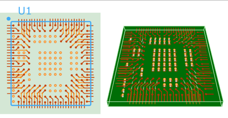
Advancements in High-Density Interconnect Systems
The landscape of electronic device design has been profoundly transformed by advancements in high-density interconnect (HDI) systems. These systems have enabled the miniaturization of components while enhancing overall performance, making them pivotal in pcb manufacturing. With the rise of complex consumer electronics, the demand for pcb manufacturing companies that specialize in HDI technology has surged. This shift is fueled by the necessity for compact designs that support multiple functionalities without compromising on quality. The intricacies of HDI designs necessitate precise pcb manufacturing processes, which incorporate innovative techniques such as laser drilling and advanced imaging methods. These advancements not only reduce pcb manufacturing costs but also improve yield rates and operational efficiency. As you engage with the latest trends and technologies, you will see how these systems facilitate quicker signal transmission and greater circuit density, which are essential for high-speed data communication. In this evolving market, understanding the dynamics of HDI systems can provide you with a competitive edge whether you are involved in a pcb manufacturing business or simply an enthusiast seeking to comprehend modern circuit design’s impact on technology.
The Role of PCBs in High-Speed Data Communication
In today’s digital era, the role of printed circuit boards (PCBs) in facilitating high-speed data communication is more critical than ever. As technology advances, you may find yourself utilizing PCBs that support the growing demands of data transfer speeds, crucial for applications like telecommunications and high-performance computing. Modern PCB manufacturing processes have significantly evolved to create designs that not only support higher frequencies but also minimize signal interference and loss.
The complexity of these boards enables them to employ high-density interconnect systems, which are essential for managing numerous connections in a compact form factor. This efficiency is often driven by technical innovations that optimize the layout and materials used in PCB production. For instance, utilizing advanced substrates and integrating vias efficiently can help you achieve better thermal management and signal integrity.
Moreover, collaborating with reputable PCB manufacturing companies can give your projects a competitive edge by ensuring high-quality standards while keeping the PCB manufacturing cost manageable. Such partnerships often lead to innovation in design methodologies, which can effectively cater to the specific requirements of high-speed applications.
To illustrate this further, consider the following table that breaks down some key aspects influencing the role of PCBs in high-speed data communication:
| Aspect | Description |
|---|---|
| Signal Integrity | Essential for maintaining clarity in data transmission |
| Thermal Management | Helps prevent overheating during operation |
| Material Selection | High-quality materials reduce losses |
| Layout Design | Optimized layout improves function and efficiency |
Through understanding these components, you realize how crucial your choice of PCB design and manufacturing approach is to achieving optimal performance in modern technology applications. Whether working within a large organization or starting a new PCB manufacturing business, ensuring effective communication through advanced PCB designs is vital for success.
Innovations Driving PCB Efficiency and Performance
The realm of pcb manufacturing has witnessed groundbreaking advancements that significantly enhance both efficiency and performance in electronic applications. Today, pcb manufacturing companies leverage cutting-edge technologies such as automated assembly and advanced materials to streamline production processes. These innovations lead to a reduction in pcb manufacturing costs, making it more accessible for businesses to incorporate high-quality PCBs into their products. For instance, the use of multilayer PCBs allows for the integration of numerous functionalities within a compact footprint, drastically improving design efficiency. Additionally, advanced testing methods during the pcb manufacturing business process ensure that each board meets stringent quality standards, resulting in enhanced reliability for end-users. The integration of smart technologies, such as AI-driven design tools, is further revolutionizing how PCBs are conceptualized and produced. By harnessing data analytics, manufacturers can now optimize layouts for improved thermal performance and signal integrity, ultimately leading to superior product outcomes. As you explore the landscape of modern electronics, it becomes evident that continued innovation in PCB technology is crucial for meeting the demands of high-speed connections and compact device designs.
Applications of Electronic PCBs in Cutting-Edge Technology
The applications of electronic PCBs in cutting-edge technology are vast and continuously evolving. From consumer electronics such as smartphones and tablets to sophisticated medical devices, the utility of PCBs is integral to modern advancements. In the automotive sector, for example, PCB manufacturing has enabled the development of highly efficient electronic control units, enhancing vehicle safety and performance. Furthermore, your understanding of pcb manufacturing companies can help you appreciate how these enterprises are pushing the boundaries with innovative design techniques that cater to specific sector needs.
The growing demand for miniaturization in devices necessitates greater efficiency in pcb manufacturing, which directly influences cost-effectiveness. By optimizing pcb manufacturing cost, businesses can design lighter, smaller products without compromising on functionality or durability. The emergence of smart technology, such as IoT devices and wearables, showcases how advanced high-density interconnect systems within PCBs improve data transfer rates and functionalities in compact spaces.
Additionally, the aerospace industry benefits greatly from these innovations, relying on high-performance PCBs for navigation systems and communication equipment. As you delve deeper into the realm of pcb manufacturing business, it’s clear that these printed circuit boards not only facilitate technological integration but also drive innovation across various fields by enabling faster production times and enhanced product performance. The future seems bright as further research into PCBs aims to explore new materials and more sustainable manufacturing practices that will shape tomorrow’s technologies.
Future Trends in PCB Design and Manufacturing
As you look toward the future of PCB manufacturing, several trends are poised to reshape the industry significantly. One prominent trend is the increasing demand for miniaturization and integration of electronic components. As technology continues to advance, PCB manufacturing companies are focusing on producing smaller, more efficient boards that can accommodate the growing number of functionalities in compact designs. This shift not only helps in reducing the overall size of devices but also minimizes energy consumption and enhances performance.
Moreover, advancements in materials science are contributing to new possibilities in PCB manufacturing. The introduction of flexible and high-performance substrates allows for greater flexibility in designs, enabling manufacturers to create more sophisticated electronic products that can bend and twist without compromising functionality. As a result, pcb manufacturing cost may see fluctuations based on these new materials; however, the potential for enhanced performance can justify these costs.
Another key trend is the integration of automation and advanced software tools within the pcb manufacturing business framework. The adoption of automated processes streamlines production, reduces human error, and increases efficiency. Coupled with sophisticated design software that enables simulation and testing before actual production, you can expect faster turnaround times while maintaining high standards of quality.
Lastly, amid increasing environmental concerns, there is a growing emphasis on sustainable practices within the industry. You may notice a shift towards eco-friendly materials and processes that reduce waste during production. This trend not only aligns with global sustainability goals but also appeals to consumers who are increasingly conscious about their environmental impact.
In summary, as you navigate through these future trends, you’ll find that innovation remains at the heart of pcb manufacturing, continually evolving to meet technological demands while aligning with broader societal goals.
Conclusion
In examining the evolution of electronic PCBs, it’s crucial to recognize the profound impact of pcb manufacturing processes on the current technology landscape. As you explore this field, understanding the dynamics of pcb manufacturing companies can help you appreciate how they contribute to high standards in design and production. The cost associated with pcb manufacturing has become increasingly efficient due to innovations in technology and processes, allowing for better resource management and reduced waste. By observing trends within the pcb manufacturing business, you will see how these companies are adapting to meet demands for more complex, multi-layered boards that enable advanced functionalities in a variety of applications. This insight into both pcb manufacturing cost and production methodologies illustrates why PCBs are not just components but are fundamental enablers of modern electronics. As you reflect on this transformative journey, consider how ongoing innovations will continue to shape not just PCBs but the entire field of electronic technology moving forward.
FAQs
When exploring pcb manufacturing, you may find yourself curious about the intricacies involved in this crucial industry. Understanding the various aspects of pcb manufacturing companies is essential, as they not only produce these vital components but also innovate practices that lead to enhanced efficiency and performance. The pcb manufacturing cost can vary based on numerous factors, including design complexity, material selection, and production volume. Thus, it’s essential to assess your specific needs and potential budgets before engaging in any projects. As you investigate options within the pcb manufacturing business, you may encounter advanced techniques that cater to high-density interconnect systems which are pivotal in today’s technology landscape. Engaging with professionals in this field can provide insights into the developments that directly affect your project’s outcome, ensuring you are well-informed and capable of making optimal decisions for any electronic endeavors.