Unlock Innovation: Custom PCB Printing and Assembly Simplified
Key Takeaways
Custom PCB printing and assembly play a pivotal role in modern electronics, offering a pathway to innovative designs and enhanced project efficiency. By leveraging tailored techniques, designers can ensure that PCB assembly processes not only meet specifications but also adapt to the evolving technological landscape. The integration of PCBA methods facilitates rapid prototyping, allowing for adjustments without the need for extensive redesigns. This flexibility is increasingly crucial in sectors where time-to-market can determine competitive advantage. Moreover, emerging technologies such as automated soldering and optimization software are streamlining assembly processes and reducing the likelihood of human error. Ultimately, embracing these innovations within custom PCB development not only fosters creativity but also enhances product functionality, ensuring that projects stand out in a saturated marketplace.
Introduction to Custom PCB Printing and Assembly
In today’s rapidly evolving technological landscape, custom PCB printing and assembly have become cornerstone elements in the development of innovative electronic products. This process not only enables engineers and designers to craft highly specialized circuit boards tailored to specific needs, but it also supports the rapid prototyping of ideas that can lead to groundbreaking advancements. The pcb assembly process integrates design intricacies with manufacturing capabilities, ensuring that each component is placed accurately and efficiently. As creativity flourishes in the electronics industry, techniques that streamline production, known collectively as pcba, are essential for navigating the complexities of modern electronics design.
One notable aspect of custom PCBs is their ability to accommodate a diverse range of applications, from consumer electronics to industrial machinery. The integration of automated manufacturing technologies has significantly reduced lead times while maintaining high standards of quality. Moreover, embracing innovations in PCB printing techniques can result in more compact designs that utilize space more effectively, ultimately enhancing overall performance.
“Incorporating advanced methods into your PCB design can dramatically improve the outcome of your projects.”
As firms seek competitive advantages, understanding the nuances between traditional methods and contemporary practices can elevate product development. Adapting to these techniques not only streamlines assembly processes but also opens doors for further exploration into contemporary electronic technologies. Thus, maintaining a focus on custom PCB printing and assembly is crucial as industries continue to evolve amid increasing demands for efficiency and creativity in electronic design.
The Importance of Custom PCBs in Modern Electronics
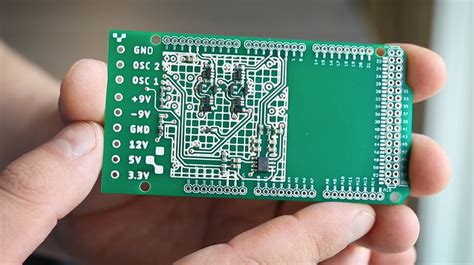
In today’s rapidly evolving technological landscape, the significance of custom PCBs (Printed Circuit Boards) cannot be overstated. These tailored solutions are essential for optimizing electronic devices, as they allow for a design that meets specific project requirements more effectively than generic options. Custom PCB printing and assembly enable engineers to create more compact, efficient, and functional devices that align with the increasing demand for innovation.
The importance of custom PCB assembly lies in its ability to enhance overall performance and reduce production costs. Unlike standard PCBs, which might not meet intricate design needs, tailor-made solutions facilitate precise layouts that can accommodate complex circuitry and multitasking components. This specificity often leads to improved signal integrity and reduced electrical noise, crucial factors in high-performance applications.
Additionally, embracing advanced pcba (Printed Circuit Board Assembly) practices can streamline manufacturing processes. By integrating innovative technologies—such as automated soldering techniques or advanced inspection systems—companies can not only enhance quality control but also minimize errors during assembly. This efficiency translates to faster turnaround times and a more agile response to market demands.
To illustrate these advantages further, consider the following table comparing traditional vs. custom PCB assembly:
| Feature | Traditional PCB Assembly | Custom PCB Assembly |
|---|---|---|
| Design Flexibility | Low | High |
| Production Cost | Higher for low volume | Optimized for scale |
| Time Efficiency | More labor-intensive | Streamlined processes |
| Quality Assurance | Moderate | Enhanced through automation |
| Suitability for Prototyping | Limited | Ideal |
In summary, the role of custom PCBs in modern electronics extends far beyond mere convenience; they represent a strategic approach to innovation and efficiency that empowers engineers and designers alike. By adopting custom designs through expert pcb assembly, companies can ensure their products not only meet current market needs but also future-proof their designs against emerging technological challenges.
Step-by-Step Guide to the PCB Design Process
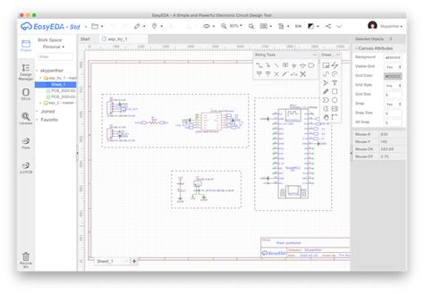
Designing a custom PCB involves a systematic approach that ensures the final product meets both functional and aesthetic requirements. The process begins with defining the specifications of the electronic circuit, where careful consideration of component selection and layout is essential. Once the specifications are established, designers typically utilize specialized software for schematic capture, which allows them to visually represent electrical connections within the circuit. This step is crucial as it serves as a blueprint for later development stages.
After creating the schematic, designers proceed to develop the PCB layout. This involves placing components on the board and routing traces to connect them according to the schematic design. During this phase, attention must be paid to signal integrity and electromagnetic interference, ensuring that all components are arranged optimally for performance.
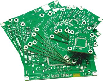
Once the layout is finalized, it’s time for PCB assembly (PCBA), where components are soldered onto the board. This step may involve hand soldering for prototypes or automated systems for mass production, helping streamline processes and enhance efficiency. The assembly stage often requires rigorous quality control measures to guarantee reliability.
Finally, after assembly, functional testing of the PCB is conducted to identify any issues before deployment. This meticulous process not only enhances creativity in electronic design but also ensures that evolving technologies in custom PCB printing and assembly continue to meet modern electronic demands efficiently. By following this systematic approach, manufacturers can overcome common design challenges, paving the way for innovative solutions in electronic production.
Innovative Techniques in PCB Printing
In today’s fast-paced technological landscape, custom PCB printing is evolving at an unprecedented rate, driven by the demand for higher efficiency and innovative designs. One of the most revolutionary techniques involves direct printing onto the substrate, which significantly reduces material waste and allows for intricate designs that were previously difficult to achieve. Furthermore, advanced ink technologies, such as conductive inks, are enabling the creation of flexible and printed electronics, making it possible to design PCBs that can bend and adapt to various applications.
Another key innovation in this area is the integration of 3D printing with traditional PCB manufacturing methods. This combination allows for rapid prototyping and the creation of complex geometries that enhance functionality without compromising performance. By utilizing integrated pcb assembly techniques within this process, designers can streamline their workflows, resulting in a more cohesive development cycle.
Moreover, software advancements play a crucial role in contemporary PCB design. With sophisticated simulation tools and artificial intelligence-driven design assistance, engineers can now predict potential challenges before physical production begins. This proactive approach not only minimizes errors but also accelerates the overall timeline for project completion.
The influence of these innovative techniques extends into pcba (printed circuit board assembly), where automation is increasingly becoming standard practice. Automated assembly lines improve precision and efficiency while reducing labor costs. Combining these new methodologies enables businesses to maintain a competitive edge while embracing creativity within electronic design.
Ultimately, as we continue to explore these burgeoning methods in custom PCB printing, engineers are empowered to push the boundaries of what is possible in electronic devices—fueling innovation that benefits industries ranging from consumer electronics to advanced robotics.
Streamlining Assembly Processes for Efficiency
In the realm of modern electronics, pcb assembly plays a crucial role in transforming intricate designs into functional products. To enhance efficiency in this process, it is essential to adopt streamlined workflows that incorporate both innovative practices and robust technologies. One effective way to achieve this is through the integration of advanced pcba techniques that simplify assembly steps, reduce time-to-market, and minimize potential errors during production. For instance, the utilization of automated assembly machines can significantly improve precision while eliminating many of the manual tasks traditionally associated with pcb assembly. Furthermore, implementing design for manufacturability (DFM) principles during the early stages of project planning contributes to a smoother assembly process by reducing complexities that can arise later on. By focusing on collaboration between design and manufacturing teams, businesses can leverage feedback loops that lead to continuous improvements in both product quality and operational efficiency. Overall, embracing these strategies not only streamlines pcb assembly, but also fosters a culture of innovation within electronic design projects, ultimately enhancing both creativity and market responsiveness.
Emerging Technologies Enhancing PCB Production
The landscape of PCB production is being transformed by the integration of emerging technologies that not only improve efficiency but also significantly enhance the quality and versatility of custom PCB printing and assembly. One prominent innovation is the use of additive manufacturing techniques, which allow for greater design freedom and reduction in waste material during the pcb assembly process. This is particularly beneficial for complex circuit designs where traditional methods may fall short. Furthermore, advancements in automation technologies streamline pcba operations, reducing manual intervention and decreasing the likelihood of human error. Additionally, incorporating machine learning algorithms can assist in predictive analysis and quality control, enabling more efficient troubleshooting during production stages. By leveraging these technologies, manufacturers can achieve higher precision in their products while simultaneously shortening production timelines. The result is a more innovative approach to custom PCB printing and assembly, driving rapid advancements in modern electronics and meeting increasing market demands for tailored solutions. As these technologies continue to evolve, they promise to further refine processes within the PCB ecosystem, facilitating a future where efficiency and creativity thrive hand-in-hand in electronic design.
Common Challenges and Solutions in PCB Design
In the realm of pcb assembly and custom electronic design, numerous challenges often emerge during the PCBA process. One prominent difficulty is ensuring the integrity and reliability of connections, which can result in failed circuits if not addressed properly. To overcome this hurdle, implementing rigorous testing methods, such as automated optical inspection (AOI) and functional testing, can significantly enhance reliability by detecting issues early in the production phase. Another challenge relates to the complexity of design, especially in high-density circuit boards where space is at a premium. Utilizing advanced software tools equipped with features like electronic design automation (EDA) can streamline the layout process while optimizing space utilization effectively. Additionally, managing component selection and availability poses issues for designers aiming to meet project timelines without compromising quality. Adopting a database-driven approach for tracking component availability ensures that alternative parts are readily identified, mitigating production delays. Ultimately, by recognizing these challenges and implementing strategic solutions, electronic designers can enhance their pcb assembly efficiency while fostering innovation throughout the design lifecycle.
Future Trends in Custom PCB Development
As we look toward the future of custom PCB development, several trends are reshaping the landscape of pcb assembly and overall design. One prominent trend is the increasing adoption of flexible PCBs, which offer enhanced versatility in applications ranging from wearable technology to advanced automotive systems. These flexible designs not only support intricate layouts but also reduce weight and improve performance. Concurrently, pcb assembly processes are being revolutionized by automation and robotics, leading to more efficient pcba production lines with minimal errors and faster turnaround times. Innovations such as 3D printing in PCB manufacturing allow for the rapid prototyping of circuits, enabling designers to iterate faster and implement complex geometries that were previously impractical. Additionally, there is a growing emphasis on integrating smart technology into PCB designs, allowing for greater functionality such as self-monitoring and data collection, which is crucial for IoT applications. Ultimately, as technologies advance and demands increase, staying informed about these emerging trends in custom PCBs will be vital for anyone involved in electronic design and production, ensuring that they remain competitive within this dynamic industry landscape.
Conclusion
In conclusion, embracing custom PCB printing and assembly can significantly enhance the efficiency and creativity of electronic design projects. The ability to tailor the PCB assembly process, often referred to as PCBA, allows engineers and designers to create more complex and innovative solutions that meet specific project requirements. By integrating state-of-the-art technologies and innovative techniques into the pcb assembly workflow, projects can be completed with greater precision and on tighter timelines. As the demand for unique electronics continues to rise, understanding how to streamline these processes will be vital for success. The journey towards effective custom PCB development not only simplifies production but also opens doors to new possibilities in electronic design innovation. Moreover, recognizing and addressing common challenges throughout the design process ensures a smoother transition from concept to finished product. Therefore, investing time in mastering these techniques will position designers at the forefront of technological advancement in electronics, making their projects not only feasible but also groundbreaking.
FAQs
What is PCB assembly?
PCB assembly (PCBA) is the process of connecting components to a printed circuit board (PCB) to create a functional electronic device. This includes the placement of electronic components, soldering them to the board, and ensuring that all connections work correctly.
Why choose custom PCB printing and assembly over standard options?
Custom PCB printing and assembly offer the ability to tailor designs specifically to project needs, enhancing both functionality and performance. This customization can lead to improved product efficiency and cost savings in the long run.
What are some common challenges in PCB design?
Common challenges include design errors, optimizing for assembly, managing component sourcing, and ensuring compliance with industry standards. Addressing these issues early in the design process can help avoid costly mistakes during production.
How long does the PCB manufacturing process take?
The duration for PCB assembly can vary based on complexity and volume. Typically, it ranges from a few days for simple boards to several weeks for more complicated designs requiring extensive testing and certification.
What technologies are emerging in PCB production?
Emerging technologies include advanced soldering techniques, automated inspection systems, and innovations in materials that enhance functionality while reducing size. These advancements allow for greater efficiency and reliability in circuitry.


