Unlocking Innovation: The Future of Additive PCB Technology
Key Takeaways
Additive PCB technology is reshaping the landscape of PCB manufacturing, offering a myriad of benefits that can significantly impact your design and production processes. One of the primary advantages is its ability to streamline rapid prototyping, enabling you to produce complex designs swiftly and efficiently. Unlike traditional methods, which often require extensive tooling and setup, additive manufacturing allows for a more flexible approach to design, making it easier for you to iterate and refine your projects. Additionally, by collaborating with experienced PCB manufacturing companies, you can effectively manage the PCB manufacturing cost, ensuring that your projects remain within budget while benefiting from the latest innovations in the field. As you explore the potential of this technology, you’ll discover that it not only fosters innovation but also opens doors for unique applications in various sectors, boosting your competitive edge in the PCB manufacturing business. Embracing these changes means you’re not just keeping pace with industry advancements but actively participating in the evolution of electronic design and production methodologies.
Understanding Additive PCB Technology: An Overview
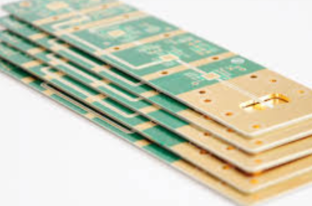
Additive PCB technology represents a significant paradigm shift in the world of PCB manufacturing. Traditionally, subtracting material from a larger piece has been the norm; however, this innovative approach allows you to add materials layer by layer, which can lead to more intricate and efficient designs. By leveraging techniques like 3D printing, this technology not only reduces waste but can also lower the PCB manufacturing costs, making it a feasible option for both small-scale projects and larger commercial enterprises.
As you delve into additive PCB solutions, it’s essential to recognize how certain PCB manufacturing companies are adapting to this shift. They are investing in advanced machinery and expertise that cater specifically to the nuances of additive techniques. This can lead to lower manufacturing costs for complex designs that would otherwise be impractical with traditional methods.
Moreover, as your understanding deepens, consider the potential applications in various sectors such as automotive and aerospace—areas where precision is paramount. The capabilities of additive manufacturing can support the creation of custom circuits suited for demanding environments.
“The road to innovation often requires embracing new methods and discarding old habits.”
In this rapidly advancing field, knowing how additive technologies complement your PCB manufacturing business strategically positions you for future growth. The emphasis on rapid prototyping also cannot be overstated; it allows for quick iterations that drive innovation while ensuring your products meet high standards without unnecessary delays. By harnessing these techniques, you prepare yourself not just for today’s market needs but also pave the way for what lies ahead in electronic design.
Advantages of Additive PCB for Rapid Prototyping
Additive PCB technology revolutionizes the landscape of pcb manufacturing, particularly when it comes to rapid prototyping. Traditional methods often involve lengthy processes and substantial costs, whereas additive manufacturing allows you to create intricate prototypes in a fraction of the time. With pcb manufacturing companies increasingly adopting this technology, you can expect faster iterations and reduced design constraints. This flexibility is crucial for testing and validating concepts before moving into full-scale production, significantly lowering the pcb manufacturing cost associated with design modifications. Moreover, the capability to manufacture highly complex geometries means that you can achieve designs that may have been impossible or too costly with conventional methods. As the industry continues to evolve, embracing additive approaches in your pcb manufacturing business not only enhances productivity but also fosters innovation, pushing the boundaries of what’s achievable in electronics design. By exploring platforms like Andwin PCBA, you can gain insights into how these advancements can directly benefit your projects.
Complex Designs Made Possible: The Power of Additive Manufacturing
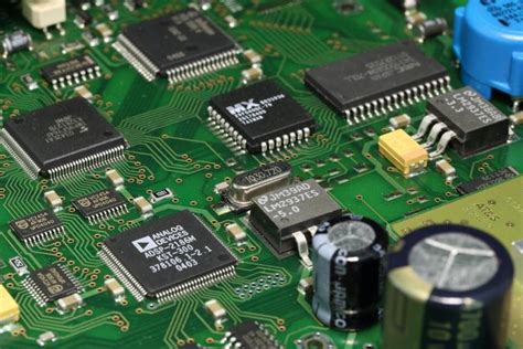
The advent of additive PCB technology has revolutionized pcb manufacturing, enabling you to create intricate designs that were previously considered impractical or impossible. This innovative approach allows you to layer materials with precision, facilitating complex geometries that traditional methods struggle to achieve. For instance, imagine integrating multiple functions into a single board; you can streamline your designs by eliminating extraneous components while ensuring functionality and efficiency. The flexibility provided by additive manufacturing means you can easily iterate and modify your designs without incurring significant pcb manufacturing costs.
To illustrate the benefits more clearly, consider the following table comparing traditional PCB production with additive methods:
| Feature | Traditional PCB Manufacturing | Additive PCB Manufacturing |
|---|---|---|
| Design Complexity | Limited | High |
| Prototyping Speed | Slower | Rapid |
| Material Waste | High | Minimal |
| Cost Effectiveness | Costly for low volumes | Economical for varying volumes |
Moreover, as you explore pcb manufacturing companies, you’ll find that many are adopting this new technology, poised to meet the demands of an increasingly complex electronic landscape. By embracing additive manufacturing, you’re not just optimizing your design process; you’re also aligning your business with future innovations in electronics that promise greater sustainability and functionality. As the industry evolves, the ability to harness advanced techniques will give you a competitive edge in this dynamic market landscape.
Current Manufacturing Processes in Additive PCB Production
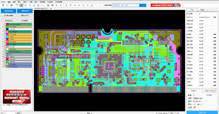
In the realm of additive PCB production, the landscape is evolving rapidly, reshaping the traditional PCB manufacturing approach. You might find that many PCB manufacturing companies are now embracing technology that streamlines and enhances production processes. The core of this evolution lies in utilizing digital design and additive techniques, which foster a level of precision and customization previously unattainable. In contrast to conventional methods, where layers are typically subtracted or etched away from materials, additive processes build materials layer by layer. This not only minimizes waste but also allows for more intricate designs that cater to specific requirements without significantly increasing the PCB manufacturing cost.
By integrating advanced printing techniques, such as inkjet or laser sintering methods, manufacturers can achieve intricate geometries and embedded components directly within the circuit. This capability opens up avenues for more innovative designs that can redefine product functionality and efficiency. For those venturing into the PCB manufacturing business, tapping into these advanced processes provides a competitive edge that can attract clients looking for swift prototypes or highly customized circuits. As you explore these innovations in your own PCB manufacturing ventures, you’ll likely come to appreciate their transformative potential—offering not only enhanced performance but also setting the stage for future developments in electronics you may want to consider.
Innovations on the Horizon: The Future of Additive PCB Technology
As you explore the realm of additive PCB technology, you will uncover a landscape rich with promise, particularly for your pcb manufacturing practices. This technology not only streamlines the process but also opens new avenues for complex designs that were once deemed impossible. By utilizing additive processes, you can embrace greater flexibility in your design approach, allowing you to significantly reduce the pcb manufacturing cost associated with traditional methods. One of the most compelling aspects of additive PCB is its effectiveness in rapid prototyping; this capability ensures that you can iterate designs swiftly without extensive tooling changes, much to the advantage of your pcb manufacturing business.
Imagine being able to create intricate geometries that accommodate multiple layers in a single build—something that traditional subtractive methods struggle with. This innovation allows pcb manufacturing companies to not only meet current demands but also anticipate future trends in electronics. As advancements continue, focusing on integrating smart materials and enhancing processes through automation may very well dictate the next steps in the evolution of additive PCB. The careful consideration of these innovations will empower you to stay ahead in a fiercely competitive market, meeting customer expectations for both quality and speed efficiently.
Case Studies: Successful Applications of Additive PCB
In recent years, numerous pcb manufacturing companies have harnessed the power of additive PCB technology to revolutionize their production processes. One notable case involved a startup that focused on creating custom electronics for the medical sector. By utilizing additive manufacturing techniques, they significantly reduced the pcb manufacturing cost associated with traditional methods, allowing them to offer highly customized solutions at competitive prices. This innovation not only expedited their pcb manufacturing business but also enhanced their ability to prototype new designs swiftly, enabling faster turnaround times for critical projects.
Another successful case is seen with a leading automotive manufacturer that adopted additive PCB technology for complex circuit designs in electric vehicles. This application has highlighted how the intricacies of modern vehicle electronics can be managed effectively using such innovative techniques. They were able to explore intricate configurations that would have been challenging and costly with conventional pcb manufacturing methods. The result was not only improved performance in their products but also a stronger market position through enhanced design capabilities.
Such examples underscore the transformative potential of additive PCB technology across diverse industries and serve as a model for how pcb manufacturing companies can stay ahead in a rapidly evolving technological landscape. Embracing these innovative processes not only addresses the challenges of today’s complex designs but also opens avenues for future advancements in electronics, positioning companies for sustainable growth.
Challenges and Solutions in Implementing Additive PCB Technologies
Implementing additive PCB technologies presents various challenges, yet solutions are continually evolving to help PCB manufacturing companies navigate these hurdles. One significant issue is the pcb manufacturing cost, which can deter smaller enterprises from adopting such advanced technologies. However, as the market matures, you will find that innovations in materials and processes often lead to a reduction in costs over time. Furthermore, technical expertise is crucial in this landscape, as you may encounter gaps in knowledge and skills specific to additive manufacturing. To address this, companies can invest in training programs or partnerships with educational institutions that focus on electronic design and pcb manufacturing techniques. The need for quality assurance also plays a vital role; implementing rigorous testing protocols will help you ensure the reliability of your complex designs and rapid prototypes. By proactively tackling these challenges with effective training and innovative processes, you can leverage the full potential of additive PCB technologies while enhancing your overall pcb manufacturing business operations.
The Integration of AI in Enhancing Additive PCB Development
As you delve into the world of additive PCB technology, it’s essential to recognize how AI is reshaping the pcb manufacturing landscape. By harnessing advanced algorithms, manufacturers can streamline the design and production phases, ultimately reducing the pcb manufacturing cost while boosting efficiency. Imagine a scenario where predictive analytics help you anticipate potential failures before they occur; this is a reality enabled by AI’s capability to analyze vast amounts of data in real-time. Furthermore, pcb manufacturing companies are increasingly adopting machine learning tools to optimize their processes, resulting in improved yield rates and overall product quality. This harmonious blend of AI and additive processes empowers you to tackle complex designs that were once deemed unfeasible. As a participant in the pcb manufacturing business, leveraging these technologies not only enhances your offerings but positions you at the forefront of innovation in a rapidly evolving industry. The transformative implications of this integration extend well beyond mere productivity gains; they pave the way for groundbreaking advancements that could redefine the very fabric of electronic component design and production.
Conclusion
As you reflect on the potential of additive PCB technology, it becomes evident that the landscape of PCB manufacturing is on the cusp of a significant transformation. With the rise of rapid prototyping and sophisticated design capabilities, this innovative approach is not just a trend; it’s reshaping how PCB manufacturing companies operate. The integration of additive manufacturing methods helps reduce the overall PCB manufacturing cost while allowing for flexibility and speed that traditional methods simply cannot match. As you consider diving into PCB manufacturing business, embracing these advancements can position you at the forefront of the industry, enhancing your competitiveness while enabling you to tackle more complex projects. The possibilities are vast, and staying informed about emerging technologies will be crucial as you navigate this evolving field. Ultimately, harnessing the power of additive PCB technology offers profound rewards—aligning your business with futuristic innovations while optimizing efficiency in production processes.
FAQs
What are the main benefits of additive PCB technology?
Additive PCB technology offers numerous benefits, such as reduced pcb manufacturing costs and the ability for rapid prototyping. This allows for quicker iterations and enhancements in designs, which is crucial for staying competitive.
How does additive manufacturing enable complex designs?
The flexibility of additive PCB processes allows for intricate geometries and multi-layer circuits that traditional methods struggle to produce. This capability opens new avenues for innovation in the pcb manufacturing business.
Can additive PCB technology reduce overall production times?
Yes, utilizing additive methods can significantly decrease production times due to streamlined processes that eliminate much of the traditional pcb manufacturing steps. This efficiency can enhance your ability to meet customer demands swiftly.
What is the expected impact of additive PCB on future innovation?
As industries evolve, additive PCB technology is poised to play a pivotal role. Innovations will likely focus on further reducing pcb manufacturing costs, improving design flexibility, and enhancing overall performance in electronic devices.
Are there any notable challenges in adopting additive PCB technologies?
While there are hurdles such as initial setup costs and the need for skilled personnel, many pcb manufacturing companies are finding effective solutions. Overcoming these barriers can lead to substantial long-term gains.