Unlocking Innovation: Your Guide to 4 Layer PCB Prototypes
Key Takeaways
In the realm of electronics, understanding 4 layer PCB prototypes is essential for any engineer or hobbyist aiming to enhance their projects. As you delve into the design and production process, keep in mind that partnering with reliable pcb manufacturing companies is crucial for ensuring quality and precision in your prototypes. Paying attention to the pcb manufacturing cost will help you budget effectively, especially when it comes to experimenting with various designs. It’s worth noting that a well-established pcb manufacturing business can offer valuable insights and services that cater to your specific needs, from initial design support to final fabrication. By navigating these key elements wisely, you can optimize your project outcomes and leverage the innovative advantages that come with 4 layer PCBs.
Introduction to 4 Layer PCB Prototypes
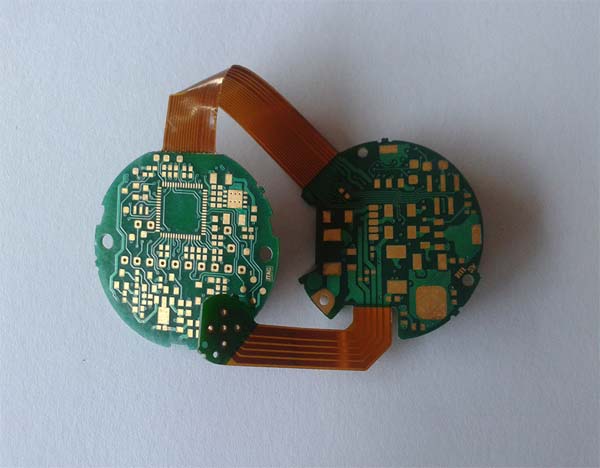
In today’s rapidly evolving technological landscape, 4 layer PCB prototypes emerge as pivotal building blocks in the development of modern electronic devices. These prototypes not only enable more complex circuit designs but also enhance performance through effective signal integrity and reduced electromagnetic interference. By integrating four conductive layers, you can create a more compact design, ultimately saving space and allowing for greater functionality in your final products.
When engaging with pcb manufacturing, it is crucial to understand the different aspects influencing your project. The pcb manufacturing cost can vary significantly depending on factors such as material selection, layer count, and fabrication techniques. Partnering with reputable pcb manufacturing companies will ensure you benefit from their expertise in producing high-quality prototypes that meet your specifications.
You may also consider the scalability of your project when diving into a pcb manufacturing business. The ability to transition from a prototype to mass production without compromising quality is vital. Keep in mind the importance of meticulous design practices; your prototype will serve as the foundation for subsequent iterations, making initial accuracy paramount.
“Investing time in thorough initial designs pays off in the long run during the manufacturing process.”
With a deep understanding of the benefits and considerations involved, you will be well-equipped to embark on your journey into the world of 4 layer PCB prototypes. Whether you’re an engineer aiming to innovate or a hobbyist eager to see your ideas materialize, recognizing these foundational elements brings you closer to achieving exceptional electronic solutions.
Advantages of 4 Layer PCBs in Modern Electronics
When it comes to pcb manufacturing, the advantages of 4 layer PCBs are numerous and critical in modern electronics. First and foremost, these boards provide enhanced functionality by allowing for an increased number of electronic components without significantly enlarging the overall dimensions of the circuit board. This compact design leads to improved performance, as signal integrity is maintained over multiple layers, which minimizes interference. Moreover, 4 layer PCBs enable better heat dissipation due to their layered architecture, a crucial factor in high-performance applications.
Another key benefit is the reduction in pcb manufacturing cost when compared to traditional two-layer boards for complex designs. Although initial expenses may seem higher due to increased complexity in the pcb manufacturing companies‘ processes, savings can be realized over time through reduced assembly costs and improved yield rates. By consolidating components onto fewer boards or layers, you can streamline your manufacturing process without sacrificing quality or performance.
Additionally, from a design perspective, using a 4 layer PCB allows for more sophisticated routing options and better ground connections which ultimately lead to greater reliability and performance of your electronic devices. This becomes increasingly important as demands for functionality continue to grow across different sectors, making pcb manufacturing businesses that specialize in multi-layer boards invaluable partners for engineers and designers striving for innovation in their projects.
In summary, adopting 4 layer PCB technology can lead not only to enhanced system performance and reliability but also present opportunities for cost-effective solutions that keep pace with the rapidly advancing world of electronics.
Key Design Considerations for 4 Layer PCBs
When embarking on the journey of designing a 4 layer PCB, there are several crucial factors to bear in mind that can significantly impact your project’s success. Thermal management is one of the primary considerations; the heat generated by components should be efficiently dissipated to prevent damage and ensure optimal performance. You must also think about the layer stack-up; how you arrange your layers affects both the electrical performance and manufacturability of your board. As you delve into circuit density, remember that 4 layer PCBs offer a balanced solution, allowing for more complex designs compared to simpler configurations, while still being less challenging than higher-layer options.
Moreover, understanding the pcb manufacturing process is essential for a smooth transition from design to production. You should actively research various pcb manufacturing companies and their processes, looking for those that provide flexibility along with exemplary quality control practices. Cost considerations cannot be overlooked either; factors such as material selection and board complexity directly influence the pcb manufacturing cost, making it vital to strike a balance between functionality and budget constraints. Lastly, ensure that both electrical and mechanical aspects are aligned with your project requirements.
In summary, a successful design of your 4 layer PCB involves a comprehensive understanding of thermal issues, careful planning around layer stack-up, thoughtful circuit density management, diligent research of pcb manufacturing partners, and an emphasis on maintaining budgetary limits while achieving design goals in your pcb manufacturing business. This holistic approach will empower you to create efficient designs that fully leverage the advantages offered by 4 layer structures.
Choosing the Right Manufacturer for Your Prototype
Selecting the right manufacturer for your 4 layer PCB prototype is a crucial step that can significantly impact both the quality of your final product and your overall pcb manufacturing cost. When assessing various pcb manufacturing companies, consider their experience in handling multi-layer designs, as this is essential for achieving optimal performance and reliability. A company with a solid track record in pcb manufacturing will not only provide high-quality prototypes but also valuable insights that can enhance your design process.
You should evaluate each potential pcb manufacturing business based on several key criteria, including their production capacity, turnaround times, and adherence to industry standards. It is also beneficial to inquire about their testing protocols to ensure your prototype meets all required specifications. The table below outlines some factors to consider when selecting a manufacturer:
| Criteria | Importance Level | Considerations |
|---|---|---|
| Experience in Multi-Layer | High | Look for previous successful projects |
| Production Capacity | Medium | Ensure they can meet your order sizes |
| Turnaround Times | High | Quick delivery can save development time |
| Testing Protocols | High | Advanced testing increases reliability |
| Customer Service | Medium | Responsive support can ease communication |
By carefully analyzing these aspects and engaging in open dialogue with potential manufacturers, you will position yourself to make an informed decision that aligns with both your project needs and budget constraints. Trusting the right pcb manufacturing company will empower you to bring your innovative designs to life with assurance and efficiency.
Step-by-Step Guide to Designing a 4 Layer PCB
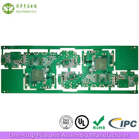
Designing a 4 layer PCB can be a transformative experience for your projects. In the initial stages, you need to focus on defining your circuit requirements. This includes selecting the appropriate components and laying out their configuration in a way that minimizes interference and optimizes performance. One of the key aspects to consider is the choice of materials; using high-quality substrates can significantly influence the electrical performance of your board.
Next, you will want to create a schematic diagram that accurately represents your design intentions. This diagram will act as a blueprint for your PCB, facilitating smoother integration during the pcb manufacturing phase. When transitioning from schematic to layout, ensure you are mindful of impedance control and signal integrity, as these factors become increasingly pertinent in multi-layer designs.
Once your layout is complete, working with pcb manufacturing companies becomes essential to bringing your design to life. It is crucial to engage with manufacturers who specialize in 4 layer PCBs, as they will be familiar with the nuances and requirements specific to such designs. During this stage, it’s necessary to communicate openly about your design specifications, including layers and dimensions, since this affects pcb manufacturing cost directly.
As you finalize your drawings, consider performing DFM (Design for Manufacture) checks to preemptively identify potential pitfalls in production. Ultimately, paying attention to these details not only streamlines the production process but also ensures that you receive a functional prototype that meets or exceeds your expectations—making it a worthwhile investment for any growing pcb manufacturing business involved in innovative electronics.
Common Challenges and Solutions in 4 Layer PCB Fabrication
When engaging in 4 layer PCB fabrication, you may encounter various challenges that can affect the performance and reliability of your designs. One significant issue is the layer alignment during the manufacturing process. Precise alignment is crucial to avoid signal integrity problems and ensure proper functionality. You can mitigate this by choosing a reputable pcb manufacturing company that employs advanced techniques such as laser-based alignment systems, which enhance accuracy. Another common challenge is managing thermal dissipation, as multi-layer boards tend to generate more heat. Incorporating thermal vias and selecting materials with better thermal conductivity can help address this issue effectively.
Additionally, the pcb manufacturing cost can be a significant concern for many engineers and hobbyists. Balancing quality with affordability often requires careful planning during the design phase. Opting for standard sizes and component layouts can reduce costs, as these practices align with the production efficiencies of many pcb manufacturing companies. Lastly, ensuring that your design meets the specified tolerances is critical. Utilizing design rule checks (DRC) in your PCB software can help you identify potential issues before sending your files for production, thereby streamlining your workflow and minimizing revisions.
Overall, while you might face challenges in 4 layer PCB fabrication, understanding these common hurdles and implementing targeted solutions will empower you to create more efficient and reliable designs for your projects.
Tips for Cost-Effective Prototyping of 4 Layer PCBs
When embarking on the journey of 4 layer PCB prototypes, one of the most important factors to consider is achieving cost-effectiveness without sacrificing quality. To start, you should explore various pcb manufacturing options that can cater to your specific needs while keeping costs manageable. Choosing materials wisely is crucial; for instance, opting for standard materials can significantly reduce your pcb manufacturing cost. Additionally, working with reputable pcb manufacturing companies that offer bulk order discounts can prove beneficial, especially if you plan to scale your production in the future. It’s advisable to be clear about your design requirements from the outset—clear specifications allow manufacturers to optimize their processes, which can lead to lower costs. You may also want to utilize prototyping tools and software that facilitate efficient design; these tools help in minimizing errors and maximizing precision during the initial developmental phases. Keep in mind that proactive communication with your pcb manufacturing business will allow you to understand the entire process and highlight any areas representing potential savings. With careful planning and attention to detail, you can create a high-quality 4 layer PCB prototype at a fraction of the expected price, enhancing both innovation and feasibility in your projects.
Future Trends in PCB Technology: The Rise of Multi-layer Designs
As you navigate the evolving landscape of PCB manufacturing, it’s essential to recognize the significance of multi-layer designs, particularly the emergence of 4 layer PCB prototypes. These innovations offer a remarkable foundation for modern electronics, merging compactness with intricate functionality. The demand for complexity in circuits has prompted many PCB manufacturing companies to adopt multi-layer configurations, enabling increased circuit density without compromising performance. In this context, understanding your PCB manufacturing cost becomes vital; multi-layer designs might initially appear pricier, but they often result in more efficient layouts and reduced board sizes that can offset expenses over time. As technology progresses, the PCB manufacturing business leans toward flexibility and adaptability, providing you with options that cater to both high-performance applications and cost-effective solutions. With this shift toward more sophisticated assemblies, keeping abreast of these trends ensures that your designs not only meet current market demands but also anticipate future developments in electronics. Embracing these advancements allows you to create projects that are both innovative and efficient, positioning yourself at the forefront of PCB technology evolution.
Conclusion
In summary, understanding the ins and outs of 4 layer PCB prototypes can play a pivotal role in elevating your projects. As you embark on the journey of pcb manufacturing, you’ll discover that collaborating with reliable pcb manufacturing companies is crucial for ensuring high-quality results. Finding the right balance between cost and quality is essential; hence, it’s important to assess the pcb manufacturing cost effectively. By doing so, you empower yourself to navigate through potential pitfalls in the pcb manufacturing business, ultimately allowing your innovations to take shape with precision and reliability. As technology advances, staying informed on best practices and emerging trends will give you a competitive advantage in this ever-evolving field. Remember, each prototype is not just a step in your design process but also a valuable learning opportunity that refines your skills as an engineer or hobbyist.
FAQs
What is the typical pcb manufacturing cost for a 4-layer prototype?
The pcb manufacturing cost for a 4-layer prototype can vary significantly based on factors such as size, complexity, and the materials used. On average, costs can range from $100 to $500 for smaller runs.
Which pcb manufacturing companies are best for prototypes?
When selecting from various pcb manufacturing companies, look for those that specialize in prototyping and have positive reviews. Companies like JLCPCB and PCBWay are often recommended due to their reliability and customer service.
How can I find the right pcb manufacturing business for my project?
To find the right pcb manufacturing business, consider factors such as lead time, capability of producing multi-layer boards, cost-effectiveness, and available support. It’s essential to check their portfolio and client testimonials to ensure they meet your requirements.
What common issues arise in pcb manufacturing, particularly for 4-layer boards?
Common issues in pcb manufacturing, especially with 4-layer boards, include layer alignment problems, incorrect drill sizes, and improper material selection. To mitigate these risks, comprehensive testing and proper design rules should be followed.