Unlocking Innovation: Your Guide to 6 Layer PCB Prototypes
Key Takeaways
In the realm of PCB manufacturing, understanding the distinct benefits of 6 layer PCB prototypes can significantly influence your design choices. These prototypes offer enhanced design flexibility, accommodating various functionalities without substantially increasing the footprint of your device. When partnered with leading PCB manufacturing companies, you can leverage these prototypes for advanced applications that demand higher density and performance. Furthermore, grasping the intricacies of PCB manufacturing cost is crucial; while multi-layer designs may be initially more expensive, they can provide long-term savings through reduced assembly and interconnection costs. In engaging with the PCB manufacturing business, you will find that the return on investment associated with 6 layer PCBs often outweighs any upfront financial considerations, particularly for high-performance electronic devices where every millimeter counts.
Unlocking the Basics: Understanding 6 Layer PCB Prototypes
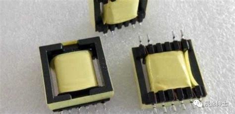
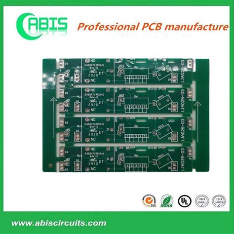
When delving into the world of 6 layer PCB prototypes, it’s essential to grasp their fundamental components and design intricacies. A 6 layer PCB consists of six conductive layers laminated together, which facilitates enhanced signal integrity and reduced crosstalk. This multi-layer structure allows for a greater number of components to be accommodated within a compact footprint, making it ideal for high-density applications. As you consider your options, it’s important to engage with the right pcb manufacturing companies that can create these advanced designs tailored to your specifications.
One significant aspect of this technology is the increased design flexibility it offers. With multiple layers at your disposal, you can strategically allocate power and ground planes, which significantly simplifies routing challenges and meets the demands of modern electronic devices. The pcb manufacturing cost for 6 layer PCBs tends to be higher than that of simpler designs due to the complexity involved in their production; however, this investment often pays off in terms of performance and functionality.
Here’s a quick comparison table on different PCB layers and their characteristics:
| Number of Layers | Advantages | Typical Applications |
|---|---|---|
| 2 | Low cost; easy to manufacture | Basic consumer electronics |
| 4 | Better performance; moderate cost | Communication devices |
| 6 | High density; advanced routing capabilities | High-end audio equipment |
“The right design can elevate your product from standard to exceptional.”
As you explore potential partners for your pcb manufacturing business, understanding these foundational elements will be vital. By prioritizing a collaborative approach with skilled professionals who specialize in 6 layer PCB prototypes, you’re setting yourself up for success in developing groundbreaking electronic solutions that meet industry demands.
Designing for Success: Key Considerations in 6 Layer PCB Layout
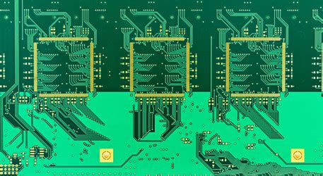
When embarking on the journey of 6 layer PCB prototypes, it is essential to understand the intricacies of designing efficient layouts. The pcb manufacturing process for such complex designs involves not just technical knowledge but also strategic planning. One of your primary concerns should be the stack-up configuration, which directly influences signal integrity and thermal management. Each layer must be meticulously arranged to minimize electromagnetic interference, particularly in high-density electronics.
Moreover, ensure that your design accommodates sufficient via sizes and spacing which are essential for maintaining connectivity and performance across layers. Choosing the right pcb manufacturing companies can significantly impact your project’s success; select those with proven expertise in consolidating multiple layers effectively. Additionally, collaborating closely with these manufacturers can streamline the design process, allowing for thoughtful adjustments that enhance layout efficiency.
As you keep an eye on pcb manufacturing cost, prioritize designs that balance complexity with functionality. While more layers may add to the expense, they also provide accrued benefits such as improved routing capabilities and enhanced performance in compact spaces—critical factors when operating within competitive markets.
Ultimately, your approach should reflect a careful consideration of these elements, designed to ensure not just the viability of your prototype but also its future adaptability within evolving technologies.
The Advantages of 6 Layer PCBs: Why Choose a Multi-layer Approach?
When considering the benefits of 6 layer PCBs, it’s essential to understand why a multi-layer approach stands out in the realm of electronic design. One of the most significant advantages is enhanced performance. The increased number of layers allows for better signal integrity, which translates to reduced electromagnetic interference and improved overall functionality. This is particularly crucial for devices requiring high-speed operation, where data transmission speeds can significantly affect performance.
Moreover, 6 layer PCBs enable greater design flexibility, enabling you to consolidate multiple functions into a smaller footprint. This can greatly reduce the overall size of your project, an important consideration in today’s compact electronic devices. Additionally, opting for pcb manufacturing with multiple layers can lead to improved thermal performance. By distributing heat across more layers, you mitigate hotspots and enhance the reliability of your system.
Furthermore, when engaging with pcb manufacturing companies, it’s worth noting that utilizing multi-layer boards can streamline production processes. This can potentially lower pcb manufacturing costs due to fewer individual components needing placement and soldering on the board. Essentially, combining various functions into a single board reduces assembly time and complexity.
Choosing a multi-layer approach also opens up avenues for advanced technologies such as blind and buried vias, which not only save space but also support higher pin counts without compromising design integrity. In summary, leveraging a pcb manufacturing business that specializes in 6 layer options positions your project for success in high-density applications while ensuring you maximize both efficiency and performance. For further insights on this technology and its implications for your projects, consider visiting Andwin PCB.
High-Density Applications: Where 6 Layer PCBs Shine
In the realm of modern electronics, 6 layer PCBs are particularly suited for high-density applications, where space is at a premium and performance is paramount. These multilayer boards allow for an intricate arrangement of components, making them ideal for devices that require a compact design without sacrificing functionality. As the demand for smaller, faster, and more efficient electronics continues to rise, pcb manufacturing techniques have evolved to meet these needs effectively. With pcb manufacturing companies increasingly adopting advanced technologies, you can take advantage of the flexibility that 6 layer designs offer, such as minimizing electromagnetic interference and optimizing signal integrity.
Additionally, the pcb manufacturing cost associated with multi-layer boards has become more competitive over time. This shift means that investing in 6 layer PCBs can lead to better performance in devices like smartphones, medical equipment, and sophisticated computing systems without dramatically inflating production expenses. By utilizing innovative design principles and materials, your projects can benefit from improved thermal management and power distribution, which are critical in high-density environments. Overall, 6 layer PCBs represent a fusion of efficiency and capability that is transforming how we think about electronic design and functionality in high-demand sectors.
Innovative Features: Exploring Free Via-in-Pad Technology
In the realm of 6 layer PCB prototypes, one of the most groundbreaking advancements is the free via-in-pad technology. This technique allows vias to be placed directly within the pads of components, vastly improving the routing efficiency and enabling tighter layouts for high-density applications. By eliminating redundant trace lengths, you can achieve better signal integrity and reduce potential interference, crucial in today’s intricate electronic designs. Additionally, while this innovative feature enhances performance, it also presents some challenges related to pcb manufacturing costs. It’s essential to weigh your options carefully: some pcb manufacturing companies may charge more for this advanced approach, but the benefits can often outweigh the expenses. When assessing your pcb manufacturing business, consider how free via-in-pad technology can elevate your project’s quality and functionality—ensuring you remain competitive in a market that constantly demands performance and innovation. Ultimately, understanding these sophisticated features is key to leveraging their full potential in your designs, ensuring that you produce reliable and efficient prototypes that meet rigorous industry standards.
Testing and Quality Assurance for 6 Layer PCB Prototypes
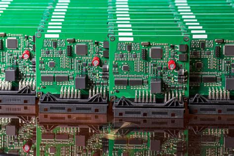
When developing 6 layer PCB prototypes, thorough testing and quality assurance are pivotal to ensure the final product meets the necessary specifications and performance standards. Various pcb manufacturing processes involve multiple stages of testing, including functional testing, electrical testing, and mechanical testing. You must engage with reputable pcb manufacturing companies that understand the importance of these quality checks. They utilize advanced technologies such as automated optical inspection (AOI) and X-ray inspection to identify potential issues at any stage of production. Ensuring reliability in your PCB is crucial, particularly as devices become more complex with high-density electronic applications. The pcb manufacturing cost can be a determining factor, but investing in proper testing can provide immense long-term value by avoiding costly failures and ensuring customer satisfaction. It is essential for anyone operating within the pcb manufacturing business landscape to prioritize these practices to maintain a competitive edge while producing high-quality prototypes capable of thriving in demanding environments.
Cost-Effective Solutions: Navigating Pricing and Production Challenges
When engaging in pcb manufacturing for your 6 layer PCB prototypes, understanding the financial landscape is crucial for optimizing your investment. The pcb manufacturing cost can be influenced by several factors including complexity, materials, and production volume. Knowing these elements allows you to make informed decisions that align your design goals with your budget. Collaborating with competent pcb manufacturing companies can also lead to competitive pricing options and streamline the production process. When evaluating potential suppliers, consider their track record in delivering quality while managing costs effectively—the right partner can truly enhance your pcb manufacturing business. By thoroughly analyzing and negotiating pricing structures, you position yourself to reap the benefits of advanced technology without compromising on cost-effectiveness. Ultimately, navigating these challenges not only ensures the success of your current projects but also sets a solid foundation for future innovations in high-density electronics.
Future Trends: The Evolving Landscape of 6 Layer PCB Technology
As you navigate the evolving landscape of 6 layer PCB technology, it’s essential to stay informed about the latest advancements and trends influencing the pcb manufacturing industry. The demand for high-performance electronics is driving pcb manufacturing companies to innovate, emphasizing the need for more complex designs capable of supporting advanced applications. You may notice a growing emphasis on integrating features such as enhanced thermal management and improved signal integrity in these PCBs. Furthermore, as you consider the pcb manufacturing cost, recognizing how these innovations contribute to overall efficiency and performance can help you make informed decisions. The shift towards just-in-time production methods in the pcb manufacturing business is also gaining traction, reflecting a move towards leaner operations that prioritize speed and adaptability. As you look ahead, understanding these trends will be vital for leveraging your PCB designs in ways that not only meet current demands but also anticipate future challenges within this dynamic field.
Conclusion
As you venture into the realm of 6 layer PCB prototypes, it becomes evident that understanding the intricacies of pcb manufacturing is vital. These prototypes not only offer significant design flexibility but also present an opportunity to enhance performance in high-density electronics. It’s important to closely consider your options among various pcb manufacturing companies, as quality plays a crucial role in achieving your project goals. Opting for 6 layer PCBs may initially present a higher pcb manufacturing cost, but the long-term benefits, such as improved reliability and functionality, often justify this investment. In the evolving landscape of technology, being part of a thriving pcb manufacturing business means incorporating advanced features and understanding market demands. The future looks promising for those who embrace these innovative solutions, ensuring you stay ahead in your endeavors. Remember, each choice you make in your prototype development can significantly impact the end product’s success in competitive fields.
FAQs
What is a 6 layer PCB prototype?
A 6 layer PCB prototype is a type of printed circuit board that consists of six conductive layers. These layers allow for increased design flexibility, enabling more complex circuitry to fit into a compact space.
What advantages do 6 layer PCBs offer over single or double-layer boards?
Using 6 layer PCBs can significantly reduce the size of your designs while enhancing performance. They provide improved signal integrity, reduced electromagnetic interference, and a higher density of components. This makes them particularly beneficial for high-performance applications where space and functionality are critical.
How do I find reliable PCB manufacturing companies?
When searching for PCB manufacturing companies, it’s important to consider their experience, reputation, and the quality of their products. Look for companies that offer thorough documentation, strong customer service, and proven track records in delivering high-quality prototypes.
What factors influence the PCB manufacturing cost?
The PCB manufacturing cost can be affected by several factors including the complexity of the design, the number of layers, materials used, and production volume. As complexity increases or specialized materials are required, costs will typically rise.
Is it advisable to customize my PCB design with unique features?
Certainly! Customizing your designs with features such as vias in pads can enhance performance and reduce space requirements. However, you should also consider any potential implications on PCB manufacturing business processes such as cost and time efficiency.