Unveiling the Benefits of HDI Multilayer PCB Technology
Key Takeaways
As you delve into the realm of HDI multilayer PCB technology, the multitude of advantages becomes evident. One of the standout features is high-density wiring, which not only maximizes space but also significantly enhances the performance of electronic devices. This increased density enables more complex circuitry on a smaller footprint, making PCB manufacturing an efficient process for modern electronics. You may find that PCB manufacturing companies are increasingly adopting this innovative technology to stay competitive in the fast-paced market.
By leveraging advanced PCB manufacturing techniques, these companies can offer products that boast improved circuitry capabilities, allowing for faster data transmission and reduced signal interference. Moreover, the innovative designs made possible by HDI boards can lead to reduced overall size without compromising functionality, an essential consideration for contemporary devices. Keep in mind that while these benefits are impressive, you will need to be aware of the PCB manufacturing costs associated with high-density designs. Understanding this financial aspect is crucial if you aim to thrive in the PCB manufacturing business.
"Investing in HDI multilayer PCBs is not just about embracing technology, it’s about future-proofing your products."
Thus, as you explore the various dimensions of HDI multilayer PCBs, you’ll find that they truly revolutionize electronic connectivity and efficiency across many applications.
Understanding HDI Multilayer PCB Technology
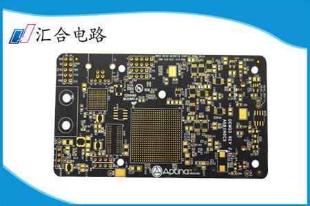
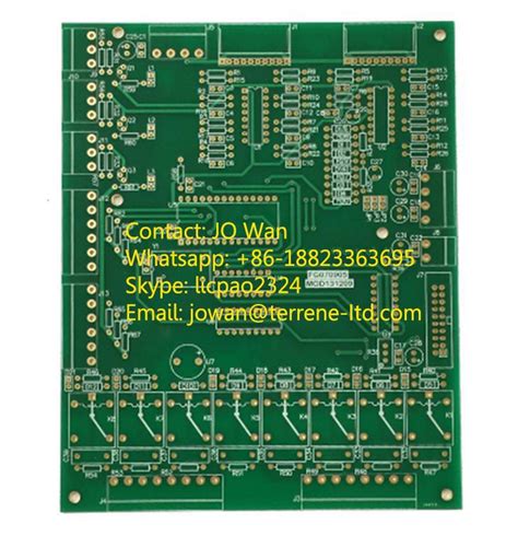
HDI (High-Density Interconnect) multilayer PCBs represent a significant advancement in the field of electronic design. Their intricate layering and compact structure allow for a greater number of connections within a smaller footprint, making them essential for modern electronic devices. In the ever-evolving landscape of pcb manufacturing, these advanced boards can accommodate densely packed features that traditional PCBs cannot support efficiently. Your design choices become more flexible as you explore pcb manufacturing companies that specialize in HDI technology, enabling the integration of various components while optimizing space utilization.
The hallmark of HDI multilayer PCBs lies in their ability to facilitate high-density wiring, which is crucial in enhancing signal integrity and reducing electromagnetic interference. This characteristic is particularly beneficial for applications where performance and reliability are paramount. The pcb manufacturing cost associated with these sophisticated boards may be higher than traditional methods, but the increase in functionality often outweighs the initial investment, particularly for cutting-edge industries such as telecommunications, medical devices, and consumer electronics.
To better understand the impact of HDI technology on pcb manufacturing business, consider the following table that outlines key features and benefits:
| Feature | Description |
|---|---|
| High-Density Routing | Enables intricate designs with reduced sizes |
| Improved Signal Integrity | Minimizes signal loss and noise during transmission |
| Flexibility in Design | Supports a variety of electronic components |
| Versatile Applications | Ideal for advanced technologies needed in various sectors |
By embracing HDI multilayer PCB technology, you’re not only enhancing your product’s performance but also positioning yourself ahead in a competitive market. As you delve deeper into its capabilities, you’ll discover how these innovations can transform your approach to pcb manufacturing and foster new opportunities for improved design outcomes.
High-Density Wiring and Its Advantages
When delving into HDI multilayer PCB technology, it’s essential to recognize the significance of high-density wiring. This advanced method allows for a more compact arrangement of electrical circuits, accommodating greater functionality within smaller spaces. As you explore the world of PCB manufacturing, you’ll find that these boards drastically reduce the physical footprint, leading to enhanced performance and efficiency in electronic devices. The compact design also translates to lower overall PCB manufacturing costs since fewer materials may be required, and the reduced size contributes to easier handling and assembly. By understanding the enhanced capabilities provided by high-density wiring, you can better appreciate how various PCB manufacturing companies utilize this technology to produce cutting-edge products. As you engage with this field, consider how adopting HDI technology can elevate your own PCB manufacturing business, making your offerings more competitive in a market that increasingly values innovation and efficiency. The shift towards high-density wiring not only optimizes connectivity but also aligns with the growing demand for reliable performance in today’s electronics.
Enhanced Circuitry Capabilities of HDI Boards
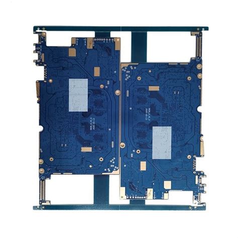
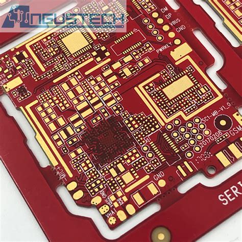
The enhanced circuitry capabilities of HDI multilayer PCBs represent a significant advancement in pcb manufacturing, allowing for the integration of more complex and compact designs. By utilizing advanced layering techniques and microvias, these boards can accommodate high-density wiring, which not only improves the electrical performance but also optimizes space, a crucial factor in modern electronic devices. As you explore the world of pcb manufacturing companies, you’ll notice that the shift towards HDI technology facilitates more intricate patterns, meaning that you can achieve higher performance levels without worrying about larger board sizes.
With lower pcb manufacturing costs per unit compared to traditional methods, investing in HDI technology is becoming more appealing for those venturing into the pcb manufacturing business. This means you can cater to a broader range of applications, from consumer electronics to sophisticated aerospace systems, thanks to the heightened reliability and functionality that HDI boards offer. Moreover, the ability to create such tailored circuit designs translates into enhanced device capabilities—resulting in faster processing speeds and increased efficiency in electronic connectivity. Embracing these innovative solutions not only meets current consumer demands but also prepares you for future advancements in technology.
Innovative Designs in HDI Multilayer PCBs
The realm of HDI multilayer PCB technology brings forth innovative designs that not only enhance the aesthetic appeal of electronic devices but also significantly improve their functionality. With the increasing demand for compact and lightweight solutions, PCB manufacturing companies are embracing these advanced techniques to produce boards that cater to modern requirements. The use of high-density wiring enables designers to incorporate more features into a smaller footprint, permitting the integration of complex circuits without the added bulk. This efficiency is critical in today’s electronic landscape, where reduced size and weight can lead to enhanced portability and performance.
Moreover, the ability to create intricate layer configurations in HDI PCBs allows for better thermal management and signal integrity. As a result, you will find that these innovative designs not only serve aesthetic purposes but also meet crucial operational demands, such as minimizing electromagnetic interference and enhancing power distribution. In evaluating the PCB manufacturing cost, it becomes clear that investing in HDI technology might initially seem higher; however, the longevity and durability of such boards can lead to cost savings in maintenance and replacements over time. By choosing HDI multilayer PCBs, you position yourself at the forefront of technology, ensuring your products remain competitive within a rapidly evolving market.
Revolutionizing Electronic Connectivity with HDI
The advent of HDI multilayer PCBs marks a significant leap in the field of electronic connectivity. With the increasing demand for devices that boast higher performance in a compact form, these boards excel by offering high-density wiring that allows for more connections in less space. This innovation is crucial for modern applications, where minimizing size while maximizing functionality is paramount. As you delve into the intricacies of pcb manufacturing, you will note that pcb manufacturing companies are now leveraging advanced techniques to enhance their production capabilities, focusing on materials and processes that facilitate higher circuit density. The pcb manufacturing cost tends to reflect this complexity; however, the benefits often outweigh the investment, as these advanced boards enable faster signal transmission and improved reliability. The extended capabilities offered by HDI technology not only revolutionize how you think about circuit designs but also shape the very future of your pcb manufacturing business, enabling it to meet the evolving demands of the electronics market. As you explore these transformations further, you’ll find that embracing HDI technology can pave the way for innovative designs that enhance connectivity across various applications.
Applications of HDI Multilayer PCBs in Modern Electronics
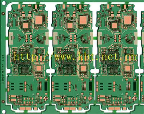
HDI multilayer PCBs have transformed the landscape of modern electronics through their versatile applications across various industries. You may find these advanced boards in compact devices such as smartphones, tablets, and wearables, where space is at a premium and connectivity needs are intensive. Their high-density wiring allows for more connections in a smaller area, thereby enhancing the overall performance and functionality of the devices. Many PCB manufacturing companies are now focusing on integrating HDI technology to meet the demands of today’s electronic market, leading to a reduction in PCB manufacturing cost through more efficient processes. Additionally, these boards play pivotal roles in automotive electronics, medical devices, and aerospace applications, where reliability and precision are crucial. By adopting HDI multilayer PCBs within your PCB manufacturing business, you not only future-proof your products but also position them at the forefront of technological advancement. Ultimately, the efficiency and innovative designs offered by HDI technology empower you to meet complex challenges while ensuring outstanding connectivity and performance in your electronic applications.
Comparing Traditional PCBs with HDI Technologies
When it comes to the pcb manufacturing process, you might find yourself weighing the differences between traditional printed circuit boards (PCBs) and HDI multilayer PCB technologies. Traditional PCBs often utilize larger trace widths and spacing, which can limit their capabilities in modern electronic applications. In contrast, HDI technologies enable significantly higher-density wiring, allowing for more connections in less space. This advancement can be vital for your projects that require compact solutions while maintaining optimal performance. Furthermore, the improved circuitry capabilities of HDI boards can lead to enhanced signal integrity and reliability, which are crucial in today’s fast-paced electronics world.
Additionally, when you consider the pcb manufacturing cost, HDI technology may initially appear higher due to the advanced processes involved. However, taking into account the long-term benefits such as reduced size and weight of your electronic devices can ultimately lead to savings that offset these initial expenses. Many pcb manufacturing companies are now embracing these innovations, resulting in more efficient products that cater to modern consumer demands.
You might also be intrigued by how HDI designs push the boundaries of what is possible in electronics. By integrating more functionality into smaller physical spaces, these boards open up new opportunities for both design flexibility and performance enhancement that traditional PCBs may struggle to provide. Thus, if you’re considering a shift in your pcb manufacturing business, leveraging HDI multilayer technology could position you favorably in a competitive market while delivering superior products that meet today’s consumer expectations.
Future Trends in HDI Multilayer PCB Developments
As you delve into the future trends of HDI multilayer PCB technology, it is essential to recognize the ongoing evolution that shapes this field. With the increasing demand for more compact and efficient electronic devices, pcb manufacturing is moving towards innovative materials and techniques. PCB manufacturing companies are investing in advanced processes that enhance performance while reducing energy consumption. This shift addresses the need for miniaturization without compromising on functionality, enabling your devices to support high-density interconnects with greater reliability. Furthermore, innovations such as embedded passive components and microvias are emerging, allowing for more complex circuitry in a smaller footprint. The pcb manufacturing cost is likely to decrease as new technologies streamline production and increase yield rates. As these advancements unfold, the pcb manufacturing business landscape will adapt, fostering a competitive environment that encourages continuous improvement and sustainability. This progression not only impacts design capabilities but also enhances how you experience connectivity in today’s fast-paced digital age.
Conclusion
In your exploration of HDI multilayer PCB technology, it’s evident that embracing high-density wiring offers numerous benefits for modern electronic applications. This revolutionary technology not only fosters enhanced circuitry capabilities but also facilitates innovative designs that can meet the demands of today’s miniaturized devices. By investing in PCB manufacturing processes tailored for HDI designs, you can significantly improve your product’s performance while optimizing overall costs. The PCB manufacturing companies that specialize in this area often deliver superior products, emphasizing quality and precision in their processes. Understanding the PCB manufacturing cost associated with these advanced techniques can also help inform your decisions in choosing the right partners for your PCB manufacturing business. By harnessing these advantages, you not only stay competitive but also pave the way for cutting-edge designs that shape the future of electronics.
FAQs
What are HDI multilayer PCBs?
HDI (High-Density Interconnect) multilayer PCBs are advanced circuit boards designed with a higher density of wiring and components. These boards offer numerous benefits, including reduced size and weight, making them ideal for modern electronics where space is at a premium.
How do HDI multilayer PCBs differ from traditional PCBs?
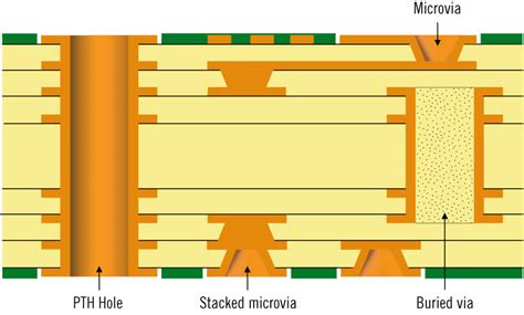
Unlike traditional PCBs, which typically have wider traces and larger pad sizes, HDI PCBs utilize micro vias, buried vias, and stacked vias. This allows for more efficient use of space and can enhance overall performance.
What advantages do HDI multilayer PCBs provide in PCB manufacturing?
The primary advantages include increased signal integrity, reduced electromagnetic interference, and better thermal management. These features lead to improved performance in complex electronic devices.
What is the typical cost of PCB manufacturing for HDI boards?
The PCB manufacturing cost for HDI boards can vary significantly based on factors such as complexity, layer count, and volume. Generally, they tend to be more expensive than standard PCB manufacturing, but the benefits often justify the investment.
What role do PCB manufacturing companies play in the development of HDI technology?
Specialized PCB manufacturing companies focus on integrating the latest technologies into their designs. They help streamline the production process to enhance quality and efficiency in developing advanced HDI boards.
For further information regarding PCB manufacturing options or to explore more about how these technologies can benefit your projects, please click here: Andwin PCB Manufacturing


