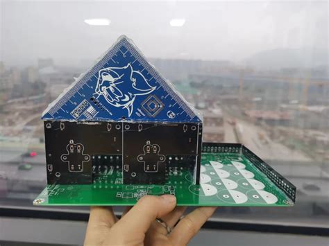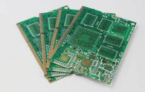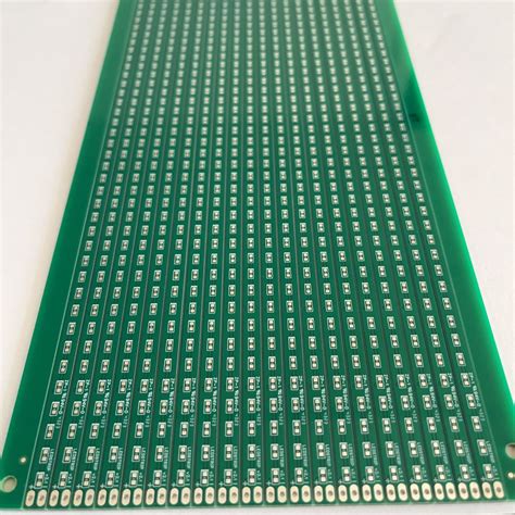
Usb 2.0 high speed pcb layout
A USB 2.0 high-speed PCB layout typically consists of several layers of copper traces and vias that connect various components and ICs on the board.
The layout is designed to minimize signal interference and ensure proper signal integrity.
The USB connector is usually located on the edge of the board and is connected to the main circuitry through a series of traces and vias.
The data lines (D+ and D-) are typically routed as differential pairs to minimize crosstalk and signal distortion.
The USB 2.0 high-speed signals require a controlled impedance transmission line,
so the traces are designed to have a specific width and spacing to maintain a consistent impedance.
The traces are also routed with proper termination to minimize reflections and signal loss.
The PCB layout also includes decoupling capacitors and other passive components to filter out noise and provide stable power to the ICs.
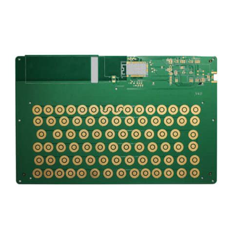
The components are placed close to the ICs they are intended to support to minimize trace length and reduce noise.
Overall, the PCB layout for USB 2.0 high-speed is designed to ensure reliable and high-speed data transfer while minimizing signal interference and distortion.

section 5 high speed pcb layout techniques
High speed PCB layout techniques are essential for designing circuits that operate at high frequencies.
These techniques are necessary to ensure that the signal integrity is maintained, and the circuit functions as intended.
Here are some of the high speed PCB layout techniques:
1. Signal Integrity:
Signal integrity is the most critical aspect of high-speed PCB layout.
It involves ensuring that the signal remains stable and free from interference.
This can be achieved by using shorter traces, minimizing the number of vias, and avoiding sharp corners.
2. Ground Planes:
Ground planes are essential for high-speed PCBs as they provide a low impedance path for return currents.
They also help in reducing electromagnetic interference (EMI) and crosstalk.
It is recommended to use a solid ground plane on the bottom layer of the PCB.
3. Power Planes:
Power planes are used to provide a low impedance path for power distribution.
It is recommended to use a solid power plane on the top layer of the PCB.
4. Component Placement:
Component placement is crucial for high-speed PCBs.
It is recommended to place high-speed components closer to the signal source and minimize the length of the traces between them.
5. Differential Pair Routing:
Differential pair routing is used for high-speed signals that require a balanced transmission line.
It involves routing two traces in parallel with a specific distance between them to maintain the impedance.
6. Controlled Impedance:
Controlled impedance is used to maintain the impedance of the transmission line.
It involves using a specific trace width, spacing, and dielectric constant to achieve the desired impedance.
7. Via Placement:
Via placement is critical for high-speed PCBs.
It is recommended to use fewer vias and place them in a way that minimizes the length of the trace between them.
8. EMI Shielding:
EMI shielding is used to reduce electromagnetic interference.
It involves placing a shield around the high-speed components or using a grounded copper pour.
In conclusion, high-speed PCB layout techniques are essential for designing circuits that operate at high frequencies.
These techniques ensure that the signal integrity is maintained, and the circuit functions as intended.
By following these techniques, designers can minimize EMI, crosstalk, and signal distortion.