Usb pcb
Designing Efficient USB PCB Layouts
Designing efficient USB PCB layouts is a critical aspect of modern electronics engineering, as it directly impacts the performance, reliability, and manufacturability of the final product. The process involves a meticulous approach to component placement, signal integrity, power distribution, and thermal management. To begin with, understanding the fundamental requirements of USB standards, such as USB 2.0, USB 3.0, and USB 3.1, is essential. Each standard has specific data rates, power delivery capabilities, and signal integrity requirements that must be adhered to during the design process.
One of the primary considerations in USB PCB layout design is the placement of components.
Proper component placement ensures minimal signal path lengths, reducing the potential for signal degradation and electromagnetic interference (EMI). For instance, placing the USB connector close to the edge of the PCB and near the associated controller can help minimize trace lengths and improve signal integrity.
Additionally, it is crucial to keep high-speed differential pairs, such as D+ and D- for USB 2.0 or the SuperSpeed pairs for USB 3.0 and above, as short and direct as possible. This practice helps maintain the characteristic impedance and reduces the risk of signal reflections.
Transitioning to the topic of signal integrity, maintaining controlled impedance for high-speed differential pairs is paramount.
Controlled impedance ensures that the signals travel with minimal distortion and loss. To achieve this, designers must carefully select the trace width, spacing, and PCB stack-up. Utilizing differential pair routing techniques, such as maintaining consistent trace separation and avoiding sharp bends, further enhances signal integrity. Moreover, incorporating ground planes beneath the signal layers can provide a return path for the signals, reducing EMI and crosstalk.
Power distribution is another critical aspect of USB PCB layout design.
USB devices often require multiple voltage levels, necessitating a well-planned power distribution network. Designers should use wide power traces or planes to minimize voltage drops and ensure stable power delivery to all components. Decoupling capacitors placed close to the power pins of integrated circuits can help filter out noise and provide a stable power supply. Additionally, implementing proper grounding techniques, such as using a solid ground plane, can further enhance the overall performance of the USB device.
Thermal management is also a vital consideration in USB PCB layout design.
High-speed USB devices can generate significant heat, which must be effectively dissipated to prevent thermal-related failures. Designers can use thermal vias, heat sinks, and copper pours to manage heat dissipation. Placing heat-generating components, such as voltage regulators and power transistors, in areas with adequate airflow can also help maintain optimal operating temperatures.
In conclusion, designing efficient USB PCB layouts requires a comprehensive understanding of USB standards, meticulous component placement, attention to signal integrity, robust power distribution, and effective thermal management.
By adhering to these principles, designers can create USB devices that perform reliably and efficiently in various applications. The integration of these considerations into the design process not only enhances the functionality of the USB device but also ensures its manufacturability and long-term reliability. As technology continues to advance, staying abreast of the latest design techniques and industry standards will be crucial for engineers striving to develop cutting-edge USB devices.
Common Mistakes in USB PCB Design and How to Avoid Them
Designing a USB printed circuit board (PCB) is a complex task that requires meticulous attention to detail. Despite the best efforts of engineers, common mistakes can still occur, potentially leading to suboptimal performance or even complete failure of the device. Understanding these common pitfalls and learning how to avoid them is crucial for ensuring the reliability and efficiency of your USB PCB design.
One of the most frequent mistakes in USB PCB design is improper trace routing.
USB signals are high-speed and require careful consideration of trace length and impedance. Failing to maintain consistent trace impedance can result in signal integrity issues, such as reflections and crosstalk, which can degrade the performance of the USB interface. To avoid this, it is essential to follow the USB specification guidelines for trace width, spacing, and layer stack-up. Additionally, using differential pairs for the D+ and D- lines and ensuring they are routed symmetrically can help maintain signal integrity.
Another common error is inadequate power supply decoupling.
USB devices often require stable power to function correctly, and any noise or fluctuations in the power supply can lead to erratic behavior or data corruption. To mitigate this, designers should place decoupling capacitors as close as possible to the power pins of the USB connector and other critical components. Using multiple capacitors of different values can help filter out a broader range of noise frequencies, ensuring a stable power supply.
Thermal management is another critical aspect that is often overlooked in USB PCB design.
High-speed USB devices can generate significant amounts of heat, which, if not properly managed, can lead to thermal throttling or even permanent damage to the components. To address this, designers should consider using thermal vias and copper pours to dissipate heat away from critical areas. Additionally, placing heat-sensitive components away from high-power areas and ensuring adequate airflow can help maintain optimal operating temperatures.
Grounding issues are also a common source of problems in USB PCB design.
A poor grounding scheme can lead to ground loops, which can introduce noise and interfere with the proper operation of the USB interface. To avoid this, designers should use a solid ground plane and ensure that all ground connections are made with low-impedance paths. Stitching vias can be used to connect different ground planes, reducing the risk of ground loops and improving overall signal integrity.
Component placement is another area where mistakes can easily occur.
Placing components too close to the USB connector can lead to mechanical stress and potential damage during insertion and removal of the USB cable. To prevent this, it is advisable to follow the recommended keep-out zones around the USB connector and ensure that components are placed with sufficient clearance. Additionally, placing critical components, such as the USB controller and associated passive components, as close to the USB connector as possible can help minimize trace lengths and improve signal integrity.
Finally, inadequate testing and validation can lead to unforeseen issues in the final product.
It is essential to thoroughly test the USB PCB design under various conditions to ensure it meets all performance and reliability requirements. This includes signal integrity testing, power supply stability testing, and thermal testing. Using simulation tools during the design phase can also help identify potential issues before the PCB is fabricated, saving time and resources in the long run.
In conclusion, avoiding common mistakes in USB PCB design requires careful attention to detail and adherence to best practices. By focusing on proper trace routing, power supply decoupling, thermal management, grounding, component placement, and thorough testing, designers can create reliable and efficient USB PCBs that meet the demands of modern electronic devices.
The Role of USB PCB in Modern Electronics
In the realm of modern electronics, the USB Printed Circuit Board (PCB) plays a pivotal role, serving as the backbone for a multitude of devices that have become integral to our daily lives. The USB PCB is a specialized type of circuit board designed to facilitate the connection and communication between various electronic components through the Universal Serial Bus (USB) interface. This interface has become a standard in the industry due to its versatility, ease of use, and ability to support high-speed data transfer.
To understand the significance of USB PCBs, it is essential to first grasp the fundamental concept of a PCB.
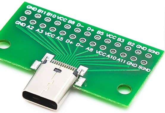
A Printed Circuit Board is a flat, typically green, board that mechanically supports and electrically connects electronic components using conductive pathways, tracks, or signal traces etched from copper sheets laminated onto a non-conductive substrate. The USB PCB, specifically, incorporates the USB interface, which allows for the seamless connection of peripherals such as keyboards, mice, storage devices, and more to a host system, typically a computer.
One of the primary advantages of USB PCBs is their ability to support multiple data transfer rates, ranging from the low-speed 1.5 Mbps to the high-speed 480 Mbps,
and even up to the super-speed 5 Gbps and beyond with USB 3.0 and USB 3.1 standards. This flexibility makes USB PCBs suitable for a wide array of applications, from simple data transfer tasks to more complex operations requiring high bandwidth. Moreover, the USB interface supports plug-and-play functionality, which simplifies the user experience by allowing devices to be connected and recognized by the host system without the need for manual configuration or driver installation.
In addition to data transfer, USB PCBs also facilitate power delivery to connected devices.
The USB standard includes specifications for power supply, enabling devices to draw power directly from the host system. This feature is particularly beneficial for portable and battery-operated devices, as it eliminates the need for separate power adapters and reduces cable clutter. The introduction of USB Power Delivery (USB PD) has further enhanced this capability, allowing for higher power transfer rates and more efficient charging of devices such as smartphones, tablets, and laptops.
The design and manufacturing of USB PCBs require meticulous attention to detail to ensure optimal performance and reliability.
Factors such as signal integrity, impedance control, and thermal management must be carefully considered during the design phase. High-speed data transfer necessitates precise control over the physical layout of the PCB to minimize signal degradation and electromagnetic interference. Advanced manufacturing techniques, such as surface-mount technology (SMT) and multi-layer PCB construction, are often employed to achieve the desired performance characteristics.
Furthermore, the integration of USB PCBs into modern electronics has driven innovation in various fields, including consumer electronics, automotive, industrial automation, and medical devices.
For instance, in the automotive industry, USB PCBs are used in infotainment systems, diagnostic tools, and charging ports for electric vehicles. In the medical field, they enable the connectivity of diagnostic equipment, patient monitoring systems, and portable medical devices.
In conclusion, the USB PCB is a critical component in the landscape of modern electronics, providing a versatile and reliable means of data transfer and power delivery. Its widespread adoption and continual evolution underscore its importance in facilitating the seamless operation of a myriad of electronic devices. As technology advances, the role of USB PCBs will undoubtedly expand, driving further innovation and enhancing the functionality of future electronic systems.
Tips for Optimizing Signal Integrity in USB PCB
When designing a USB printed circuit board (PCB), ensuring optimal signal integrity is paramount to achieving reliable performance and compliance with USB standards. Signal integrity refers to the quality and reliability of electrical signals as they travel through the PCB, and it can be affected by various factors such as impedance mismatches, crosstalk, and electromagnetic interference (EMI). To optimize signal integrity in USB PCBs, several key considerations and best practices should be followed.
Firstly, maintaining controlled impedance is crucial for USB signal integrity.
USB signals are high-speed differential pairs, and any impedance mismatch can lead to signal reflections and degradation. To achieve controlled impedance, it is essential to carefully design the trace width, spacing, and stack-up of the PCB. Utilizing a four-layer PCB stack-up with dedicated ground and power planes can help maintain consistent impedance and reduce noise. Additionally, using differential pair routing techniques, such as maintaining equal trace lengths and minimizing skew, can further enhance signal integrity.
Another important aspect is minimizing crosstalk between adjacent signal traces.
Crosstalk occurs when signals on one trace couple into another, causing interference and potential data corruption. To mitigate crosstalk, it is advisable to maintain adequate spacing between high-speed USB traces and other signal traces. Implementing ground planes and using ground vias to create a solid return path for signals can also help reduce crosstalk. Furthermore, avoiding parallel routing of high-speed traces over long distances can minimize the risk of crosstalk.
Electromagnetic interference (EMI) is another critical factor that can impact USB signal integrity.
EMI can be generated by various sources, including power supplies, switching regulators, and other high-frequency components. To reduce EMI, it is essential to implement proper grounding and shielding techniques. Placing decoupling capacitors close to the power pins of USB connectors and ICs can help filter out high-frequency noise. Additionally, using ferrite beads and common-mode chokes on power and signal lines can further suppress EMI.
Transitioning to the layout phase, careful component placement is vital for optimizing signal integrity.
Placing USB connectors and related components close to the edge of the PCB can minimize trace lengths and reduce signal degradation. Ensuring that differential pairs are routed symmetrically and avoiding sharp bends can also enhance signal quality. Moreover, placing critical components such as USB transceivers and controllers in close proximity to each other can reduce the risk of signal degradation due to long trace lengths.
Thermal management is another consideration that can indirectly affect signal integrity.
Excessive heat can cause signal distortion and affect the performance of USB components. To address this, it is important to implement proper thermal management techniques, such as using thermal vias, heat sinks, and adequate copper pours to dissipate heat effectively. Ensuring that the PCB operates within the specified temperature range can help maintain signal integrity and overall reliability.
In conclusion, optimizing signal integrity in USB PCBs requires a comprehensive approach that encompasses controlled impedance, crosstalk mitigation, EMI reduction, careful component placement, and effective thermal management. By adhering to these best practices, designers can ensure that their USB PCBs deliver reliable performance and meet the stringent requirements of USB standards. As technology continues to advance and data transfer speeds increase, maintaining signal integrity will remain a critical aspect of USB PCB design, necessitating ongoing attention and refinement.


