What are high speed signals in pcb
Understanding High Speed Signals In PCB Design
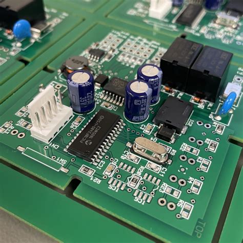
High speed signals in printed circuit board (PCB) design are a critical aspect of modern electronics, particularly as devices become more complex and demand faster data transmission rates. Understanding these signals is essential for engineers and designers to ensure the reliability and performance of electronic systems.
High speed signals refer to electrical signals that switch at high frequencies, typically in the range of hundreds of megahertz (MHz) to several gigahertz (GHz). These signals are prevalent in applications such as telecommunications, computing, and consumer electronics, where rapid data transfer is paramount.
One of the primary challenges associated with high speed signals is signal integrity.
As the frequency of the signals increases, various factors can degrade the quality of the signal, leading to errors and reduced performance. Signal integrity issues can arise from several sources, including impedance mismatches, crosstalk, and electromagnetic interference (EMI). Impedance mismatches occur when the characteristic impedance of the transmission line does not match the impedance of the source or load, causing reflections that can distort the signal. To mitigate this, designers must carefully control the impedance of the traces on the PCB through precise layout and material selection.
Crosstalk is another significant concern in high speed PCB design.
It occurs when a signal on one trace induces an unwanted signal on an adjacent trace, potentially leading to data corruption. To minimize crosstalk, designers can employ techniques such as increasing the spacing between traces, using differential signaling, and incorporating ground planes to provide a return path for the signals. Differential signaling, in particular, is effective because it uses two complementary signals that can cancel out noise and reduce susceptibility to external interference.
Electromagnetic interference (EMI) is a pervasive issue in high speed PCB design, as high frequency signals can radiate electromagnetic energy that interferes with other components and systems.
To address EMI, designers can use shielding techniques, such as enclosing sensitive components in metal cases or using ground planes to absorb and redirect electromagnetic energy. Additionally, proper grounding and decoupling strategies are essential to minimize EMI and ensure stable operation.
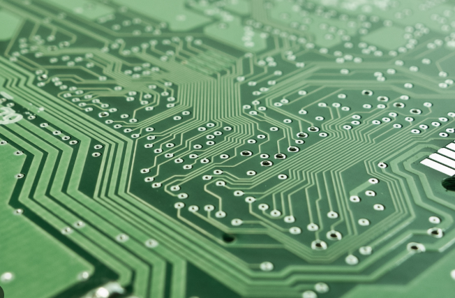
The physical layout of the PCB also plays a crucial role in managing high speed signals.
Trace length, width, and routing must be carefully considered to avoid signal degradation. For instance, longer traces can introduce delays and increase the likelihood of signal reflections, while narrower traces can increase resistance and cause signal attenuation. Designers often use techniques such as controlled impedance routing, matched trace lengths, and via minimization to optimize signal paths and maintain signal integrity.
Moreover, the choice of materials for the PCB substrate can significantly impact high speed signal performance.
Materials with low dielectric constant and low loss tangent are preferred, as they reduce signal attenuation and dispersion. Common materials used in high speed PCB design include FR-4, Rogers, and other advanced laminates that offer superior electrical properties.
In conclusion, understanding high speed signals in PCB design is essential for creating reliable and high-performance electronic systems. By addressing signal integrity issues, such as impedance mismatches, crosstalk, and EMI, and by carefully considering the physical layout and material selection, designers can ensure that high speed signals are transmitted accurately and efficiently. As technology continues to advance, the importance of mastering high speed PCB design will only grow, making it a vital skill for engineers and designers in the electronics industry.
Key Challenges Of High Speed Signals In PCB Layout
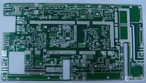
High-speed signals in printed circuit board (PCB) layout present a unique set of challenges that require careful consideration and meticulous design practices. As electronic devices continue to evolve, the demand for faster data transmission rates has increased, necessitating the use of high-speed signals. These signals, typically characterized by their rapid rise and fall times, can introduce a variety of issues that can compromise the performance and reliability of the PCB if not properly managed.
One of the primary challenges associated with high-speed signals is signal integrity.
Signal integrity refers to the preservation of the quality and shape of the signal as it travels through the PCB. High-speed signals are particularly susceptible to degradation due to factors such as impedance mismatches, crosstalk, and electromagnetic interference (EMI). Impedance mismatches occur when the characteristic impedance of the transmission line does not match the impedance of the source or load, leading to signal reflections that can distort the signal. To mitigate this, designers must carefully control the impedance of the traces by considering factors such as trace width, spacing, and the dielectric properties of the PCB material.
Crosstalk, another significant challenge, arises when a signal on one trace induces an unwanted signal on an adjacent trace.
This can be particularly problematic in densely packed PCBs where traces are in close proximity. To minimize crosstalk, designers can employ techniques such as increasing the spacing between traces, using differential signaling, and incorporating ground planes to provide a return path for the signals. Additionally, careful routing of high-speed signals can help reduce the likelihood of crosstalk.
Electromagnetic interference (EMI) is also a critical concern in high-speed PCB design.
High-speed signals can generate electromagnetic fields that can interfere with other components and signals on the PCB, as well as with external devices. To address EMI, designers can use shielding techniques, such as placing ground planes or metal enclosures around sensitive areas, and implementing proper grounding and decoupling strategies. Furthermore, the use of controlled impedance traces and differential pairs can help reduce the generation of EMI.
Another challenge in high-speed PCB design is managing power distribution.
High-speed circuits often require stable and clean power supplies to function correctly. Power integrity issues, such as voltage drops and noise on the power rails, can adversely affect the performance of high-speed signals. To ensure power integrity, designers can use techniques such as decoupling capacitors, power planes, and proper placement of power and ground vias. These measures help to maintain a stable power supply and reduce noise.
Thermal management is also a crucial aspect of high-speed PCB design.
High-speed components can generate significant amounts of heat, which can affect the performance and reliability of the PCB. Effective thermal management strategies, such as using thermal vias, heat sinks, and proper component placement, are essential to dissipate heat and maintain optimal operating temperatures.
In conclusion, the key challenges of high-speed signals in PCB layout encompass signal integrity, crosstalk, electromagnetic interference, power distribution, and thermal management. Addressing these challenges requires a comprehensive understanding of high-speed design principles and the implementation of best practices to ensure the performance and reliability of the PCB. As technology continues to advance, the importance of mastering these challenges will only grow, making it imperative for designers to stay informed and adept in high-speed PCB design techniques.
Techniques For Managing High Speed Signals In PCB
High-speed signals in printed circuit boards (PCBs) are a critical aspect of modern electronic design, particularly as devices become more complex and demand faster data transmission rates. These signals, typically characterized by their rapid rise and fall times, can introduce a range of challenges that must be meticulously managed to ensure the integrity and performance of the overall system. Effective techniques for managing high-speed signals in PCBs are essential to mitigate issues such as signal degradation, electromagnetic interference (EMI), and crosstalk.
One fundamental technique for managing high-speed signals is the careful design of the PCB layout.
The layout must be optimized to minimize signal path lengths and avoid unnecessary bends, which can cause signal reflections and loss. Utilizing controlled impedance traces is another critical aspect, as it ensures that the signal maintains its integrity over the transmission path. Controlled impedance is achieved by carefully designing the trace width, spacing, and the dielectric properties of the PCB material.
In addition to layout considerations, proper grounding is paramount in managing high-speed signals.
A solid ground plane can significantly reduce noise and EMI by providing a low-impedance return path for the signals. This helps to maintain signal integrity and reduces the potential for crosstalk between adjacent traces. Furthermore, the use of ground vias and stitching vias can enhance the effectiveness of the ground plane by providing multiple return paths and reducing loop areas.
Another technique involves the use of differential signaling, which is particularly effective in high-speed applications.
Differential pairs consist of two complementary signals that are routed together, with one signal being the inverse of the other. This approach helps to cancel out common-mode noise and reduces EMI, as the electromagnetic fields generated by the two signals tend to cancel each other out. Careful attention must be paid to the routing of differential pairs to ensure that they are closely coupled and maintain consistent spacing throughout their path.
Signal integrity can also be improved through the use of termination techniques.
Proper termination helps to match the impedance of the transmission line to the load, thereby reducing reflections and signal degradation. Common termination methods include series termination, parallel termination, and AC termination, each with its own advantages and considerations depending on the specific application and signal characteristics.
Moreover, the selection of appropriate PCB materials plays a crucial role in managing high-speed signals.
High-frequency laminates with low dielectric constant and low loss tangent are preferred for high-speed designs, as they help to minimize signal attenuation and dispersion. The choice of materials must be aligned with the specific requirements of the application, taking into account factors such as signal frequency, thermal performance, and mechanical properties.
Lastly, simulation and modeling tools are invaluable in the design process for high-speed PCBs.
These tools allow designers to predict and analyze the behavior of high-speed signals, identify potential issues, and optimize the design before physical prototyping. By leveraging simulation software, designers can experiment with different layout configurations, termination schemes, and material choices to achieve the best possible performance.
In conclusion, managing high-speed signals in PCBs requires a comprehensive approach that encompasses careful layout design, effective grounding, differential signaling, proper termination, material selection, and the use of advanced simulation tools. By employing these techniques, designers can ensure that high-speed signals are transmitted with minimal degradation, thereby enhancing the overall performance and reliability of electronic systems.
Importance Of Signal Integrity In High Speed PCB Design
In the realm of modern electronics, the importance of signal integrity in high-speed PCB design cannot be overstated. As technology advances, the demand for faster and more efficient electronic devices continues to grow, necessitating the development of high-speed signals in printed circuit boards (PCBs). High-speed signals, typically defined as those operating at frequencies above 50 MHz, are crucial for the performance of contemporary electronic systems. However, the integrity of these signals must be meticulously maintained to ensure the reliable operation of the device.
Signal integrity refers to the quality and reliability of electrical signals as they travel through a PCB.
In high-speed PCB design, maintaining signal integrity is paramount because any degradation can lead to data corruption, timing errors, and overall system failure. Several factors contribute to signal integrity issues, including signal reflection, crosstalk, and electromagnetic interference (EMI). Therefore, understanding and mitigating these factors is essential for successful high-speed PCB design.
One of the primary challenges in maintaining signal integrity is signal reflection.
When a signal encounters a discontinuity in the transmission line, such as a change in impedance, a portion of the signal is reflected back towards the source. This reflection can interfere with the original signal, causing distortion and potential data errors. To minimize signal reflection, designers must carefully control the impedance of the transmission lines by selecting appropriate materials and maintaining consistent trace widths and spacing.
Crosstalk is another critical concern in high-speed PCB design.
Crosstalk occurs when a signal in one trace induces an unwanted signal in an adjacent trace, leading to interference and potential data corruption. To mitigate crosstalk, designers can employ techniques such as increasing the spacing between traces, using differential signaling, and incorporating ground planes to provide a return path for the signals. Additionally, careful routing of high-speed signals can help minimize the risk of crosstalk.
Electromagnetic interference (EMI) is a further challenge that can compromise signal integrity in high-speed PCB design.
EMI occurs when external electromagnetic fields disrupt the signals on the PCB, leading to noise and potential data errors. To reduce EMI, designers can use shielding techniques, such as placing ground planes and metal enclosures around sensitive components. Additionally, proper grounding and decoupling strategies can help mitigate the effects of EMI on high-speed signals.
Moreover, the choice of materials plays a significant role in maintaining signal integrity.
High-speed PCBs often require materials with low dielectric constants and low loss tangents to minimize signal attenuation and dispersion. Selecting the right materials ensures that the signals can travel through the PCB with minimal degradation, preserving their integrity.
Furthermore, the layout and routing of high-speed signals are critical factors in maintaining signal integrity.
Designers must follow best practices, such as keeping trace lengths as short as possible, avoiding sharp bends, and using controlled impedance traces. Additionally, the use of simulation tools can help identify potential signal integrity issues early in the design process, allowing for timely adjustments and optimizations.
In conclusion, the importance of signal integrity in high-speed PCB design is undeniable. As electronic devices continue to evolve and demand higher performance, maintaining the integrity of high-speed signals becomes increasingly critical. By understanding and addressing factors such as signal reflection, crosstalk, EMI, material selection, and layout considerations, designers can ensure the reliable operation of high-speed PCBs. Ultimately, meticulous attention to signal integrity is essential for the success of modern electronic systems, enabling them to meet the ever-growing demands of today’s technology-driven world.