What are some high-speed PCB design tips?
High-speed PCB design refers to any design where signal integrity begins to be impacted by the physical characteristics of the PCB,such as layout,packaging,interconnects,and layer stackup. Furthermore,when you begin designing a board and encounter issues like delay,crosstalk,reflection,or emissions ,you enter the realm of high-speed PCB design.
This focus on these issues makes high-speed design unique.You may be accustomed to designing a simple PCB,focusing primarily on component placement and routing.However,with high-speed design,it’s even more important to consider factors like their distance from the signal,signal width,where to place traces factors into account will take your PCB design process to next level.
High-speed PCB design tips
1.Know Design Software That offer Advanced Options
It takes a lot of sophisticated feature to perform high-speed design in CAD software.Furthermore,there aren’t many programs specifically designed for amateurs,and they often lack the advanced options found in web-based software packages.Therefore,you need to have a better understanding of powerful CAD tools.
2.High-Speed Routing
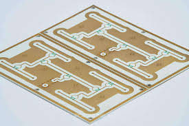
When it comes to high-speed routing,designers need to understand basic routing rules,including not cutting ground planes and keeping traces short.Therefore,digital lines should be protected from crosstalk at a certain distance and shielded from any interference sources to prevent signal integrity impairment.
3.Impedance-Controlled Traces
For certain signals,approximately 40-120ohms,Impedance matching is required.Antennas and many differential pairs are examples of characteristic impedance matching.
It is important for designers to understand how to calculate trace width and the necessary impedance values can severely impact the signal,leading to data corruption.
4.Length-Matched Traces
High-speed memory buses and interface buses have many lines.There lines can operate at very high Frequencies,so it is crucial that the signal travels from the transmitter to the receiver simultaneously.This also requires a function known as length matching.Therefore, the most common standards define tolerance values for length matching.
5.Minimize Loop Area
High-speed PCB designer need to understand several techniques.High-frequency signals can cause EMI,EMC and other problems,Therefore,they need to adhere to basic rules,such as maintaining a continuous ground plane,reducing loop area by optimizing trace current return paths, and incorporating numerous stitching vias.

High-speed PCB design Considerations
PCB Layout is important
Efficient PCB manufacturing for high-speed circuit is undoubtedly crucial to the final result.However,PCB layout is often overlooked during this process,this can significantly impact the design,ensuring the necessary functionality and successful PCB manufacturing.These factors include careful planning and adherence to key considerations .Furthermore,prior to PCB layout ,several issues must be addressed,such as design for manufacturing(DFM)practies and additional cosiderations for high-speed PCB requirements.
poor layout can lead to performance issues during testing or PCB manufacturing.Even worse,the need to evaluate PCB failures or performance issues and reassemble prototype layouts can lead to costly and time-consuming redesigns or rework.
PCB Design Consideration
High-speed PCB design Place significant constraints on designers,as they must meet various signal speed and other design requirements.Therefore,to achieve a high speed PCB design as shown below,several factors need to be cosidered:
Schematic Consideration:It’s well-known that a good schematic provides a good foundation for PCB design.Therefore,depending on whether you’re a pcb designer or an electrical engineer,you approach the schematic differently.Typically,the schematic differently,Typically,the schematic is considered a communication method that connect to the board. However,the schematic can have a significant impact on the organization and presentation of your high-speed design.Therefore,it’s important to include as much information as possible on the design schematic,such as trace lengths,necessary component placement,PCB manufacturer information,and so on.
Trace Length Adjustment:When using high-speed interfaces,you need to adjust trace lengths to synchronize signal transmission with the data lines.However,this interface may fail at the maximum frequency or not function at all due to lack of synchronization.Furthermore,the higher the interface frequency,the stricter the length matching requirements.Therefore,in the case of parallel interfaces,you only need to adjust the length of all trace ,It’s important to adjust these trace lengths to achieve the desired length for a given signal group.
PCB Material and High-speed Stackup Requirements:This will impact your high-speed design,such as the layer stackup structure and PCB material.
High-speed Placement Strategies:Because changing pad size and component clearance can minimize high-speed connection lengths,high-speed designs can employ a variety of methods to optimize component placement and improvement footprints for high speeds.
Differential Pair and Trace length Routing:Routing differential pairs in high-speed designs is crucial so that paired signals can coexist.
Crosstalk,Impedance Control and parallelism considerations:In high-speed designs,many factors can negatively impact your design.Furthermore,there are several techniques to consider,such as how to minimize these impacts.
Understanding Stripline and Microstrip: High-speed designs often requires using specific shapes or topologies. Furthermore,exploring various methods to track trace lengths, escapes,requires a good understanding of stripline and microstrip routing techniques.
Route Topologoies and best routing Practices:Achieving the circuit path required for high-speed routing often requires using specific shapes or topologies. Furthermore,exploring various methods to track trace lengths,escapes ,return paths,and so on is beneficial.
Simulator:For high-speed designs,simulations can be very beneficial before ,during,and after layout.Therefore,you should develop a better understanding of PCB design software to learn tips and tricks for analog design.
How do you know if you need high-speed designs?
1.Are there high-speed interfaces on your board?
A quick way to find out if you need to adhere to high-speed design guidelines is to check if you have high-speed design guidelines is to check if you have high-speed interfaces such as DDR,PCI-Express,or even video interfaces like DVI and HDMI.
all of these interfaces require adherence to certain high-speed design rules.Furthermore, please provide accurate specification for each in the documentation.
2.Trace Length to signal Wavelength Ratio
Generally,if the wavelength of your signal is the same as the trace length, your PCB definitely requires high-speed design.This is because some standards (such as DDR)require trace lengths to match minimum tolerances.
A good rough guideline is if your trace length and wavelength can be controlled within an order of magnitude of each other.Then,it’s best to check for high-speed design.
3.PCBs with Wireless Interfaces
As you know, every PCB has an antenna, whether through a connector or something on the board, and high-speed signals need to be designed. Furthermore, onboard antennas also require close impedance matching for tuning length.
Boards with SMA or similar connectors need to be connected to connectors with specific impedance values.
Conclusion
In short, learning about high-speed PCB design relies on engineering. While there are many factors to consider when designing high-speed PCBs, your CAD software for PCB design will provide assistance, such as impedance calculators, trace length reporting options, differential pair routers, and other tools.