What are some of the implications of the Hall Effect for PCB layout?
For me, one of the coolest things about kids is that they can be astounded by science and other phenomena that, as an adult, you are just accepting. I gave a five-year-old homemade magnetic slime for his birthday one year; consisting of iron oxide powder, Elmer’s glue, and liquid starch, the prospect of the black goo delighted everyone except the boy’s mother.
No one could question the fun of mixing the stuff or the joy. Hold up a black finger. Everyone was amazed when the clay actually followed the neodymium magnet. You could certainly feel everyone’s imaginations being reignited by the magic of the magnetic slime.
In my experience, I encounter similar forms of magnetism when understanding how to best utilize magnetic forces in my circuit board designs. Understanding Hall Effect applications will be able to keep your designs triggering your imagination. Revisiting the Hall Effect might even revisit your memories of magnetic toys.
Hall Effect!
A transverse magnetic field applied to a current-carrying conductor induces an electric field. The resulting potential difference produces a very small voltage, called the Hall voltage, that depends on the materials, current, and magnetic field.
The basic Hall sensor detects the presence of a magnetic field. Variations of the basic model are available as switches, latches, and sensors.
A Hall-effect switch opens in the presence of a transverse magnetic field and closes when the field is removed. Remove the magnetic field from a Hall-effect latch and the latch will remain open. The latch closes in the presence of a parallel magnetic field or when the power is turned off.
A Hall-effect sensor outputs an analog voltage proportional to the applied magnetic field.
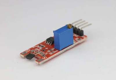
Let’s look at a few Hall-effect ICs
Addressing the challenges involved with Hall-effect sensors and PCB design begins with understanding some example operations of Hall-effect ICs.
- Sensitive, low-power, low-noise sensor ICs operate in battery-powered mobile applications that require high energy efficiency and minimal PCB space. In this example, either a north or south pole triggers IC operation. Not tying magnetic polarity to circuit operation reduces cost and simplifies installation.
Average current consumption remains low because the accompanying timing circuitry only allows power to be applied for short periods of time. The circuit remains closed during the duty cycle.
Hall-effect iterations can be seen through many different displays
- The ultra-low power Hall latch sensor can be used as a brushless DC motor sensor, mechanical travel sensor, and to measure fluids in portable medical devices, e-bikes, and flow meters. The circuit uses a pin-selectable sampling rate to monitor changes in motion.
During operation, the device responds to a magnetic field applied perpendicular to the top of the package. Placing a south magnetic pole near the top of the package causes the magnetic flux to propagate from the bottom to the top and establish a positive polarity. From this, the magnetic threshold operating point rises until the threshold is exceeded. As a result, the circuit produces a low voltage.
Applying a north magnetic pole pushes the magnetic threshold release point above the threshold and causes the circuit to produce a high voltage at the output. Alternating north and south poles toggle the output.
- Based on conventional CMOS technology, the integrated magnetic field sensor uses the Hall effect to sense current. In this design, an additional ferromagnetic layer acts as a flux concentrator and provides high magnetic gain. With this approach, the circuit remains extremely sensitive to any magnetic field parallel to its surface and produces a linear output voltage proportional to the magnetic field. The circuit includes high voltage isolation from the current conductor on the PCB and operates with low noise and low offset.
Shielded!
Each example Hall effect sensor has high sensitivity to magnetic fields. Stray external magnetic fields can cause inaccurate measurements. PCB design can prevent external magnetic fields through several methods.
You can prevent magnetic field interference by covering the device package with a surface mount magnetic shield. Although the shield shunts external magnetic flux away from the package, it does not affect the magnetic field generated within the package around the primary current-carrying path. Secure the shield to the PCB with epoxy.
Hall devices are not sensitive to magnetic flux lines parallel to their plane. Therefore, you can leave both sides of the shield open. If the circuit requires additional shielding from external perpendicular magnetic flux, place a second shield on the bottom of the PCB.
The shield may look bulky, but it is safer than damaging the PCB with it.
Space Traces
Orient high-current conductors close to the device perpendicular to the plane of the PCB. With this orientation, you let the magnetic flux circulate within the plane of the Hall device instead of through the component. As a result, flux has little or no effect on the Hall IC output. Although there are space limitations, you can protect the Hall device from interference by keeping as much space as possible between the device and other current-carrying traces.
Getting more input and involved in the process of understanding the Hall Effect and magnetic fields has completely changed my creative passion for PCB design. However, without powerful PCB design software that can meet my creative needs, my designs would go nowhere. Thankfully, Altium’s Circuit Studio® is able to handle any requirements I have in terms of layout, rule checking, and providing intelligent schematic and footprint creation software.