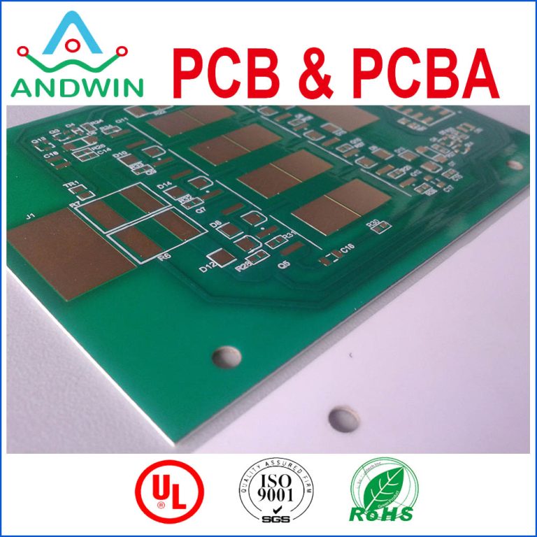
What are the common errors in PCB design?
Electronic engineers refer to senior engineering and technical personnel engaged in research, teaching, product design, scientific and technological development, production and management of various electronic equipment and information systems. They are generally divided into hardware engineers and software engineers.
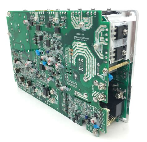
Hardware engineers: mainly responsible for circuit analysis and design; and use computer software as a tool for PCB design, and test and debug after the factory PCB is completed and the electronic components are welded;
Software engineers: mainly responsible for the writing and debugging of embedded programs such as single-chip microcomputers, DSP, ARM, FPGA, etc. FPGA programs sometimes belong to the scope of work of hardware engineers.
People make mistakes, let alone engineers? Although the world has changed, engineers often make the same mistakes! Now, please check your seat and see if you have been tricked.
It doesn’t matter what value these pull-up/pull-down resistors use, just choose an integer of 5K
Comment: There is no 5K resistance value on the market. The closest one is 4.99K (accuracy 1%), followed by 5.1K (accuracy 5%), which costs 4 times and 2 times more than 4.7K with 20% accuracy. The resistance values of 20% accuracy resistors are only 1, 1.5, 2.2, 3.3, 4.7, and 6.8 (including integer multiples of 10); similarly, the capacitors with 20% accuracy also have only the above values. If other values are selected, higher accuracy must be used, and the cost will be multiplied several times, but it will not bring any benefits.
This part of the circuit will not have any problems as long as the software is designed in this way
Comment: Many electrical characteristics of the hardware are directly controlled by the software, but software often has accidents, and it is impossible to predict what operations will occur after the program runs away. Designers should ensure that no matter what operations the software performs, the hardware should not be permanently damaged in a short period of time.
This logic can be built with 74XX gate circuits, but it is too rustic. It is better to use CPLD, which looks more high-end.
Comment: 74XX gate circuits are only a few cents, while CPLD costs at least dozens of yuan. The cost has increased N times, and it also adds several times of work to production, documentation, etc.
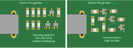
The PCB design requirements of this board are not high, so just use thinner wires and automatically route them.
Comment: Automatic routing will inevitably occupy a larger PCB area and generate many times more vias than manual routing. In large-volume products, the factors that PCB manufacturers consider for price reductions are not only business factors, but also line width and the number of vias. They affect the yield rate of PCB and the number of drill bits consumed, respectively, saving the supplier’s cost, and finding a reason for price reduction.
Our system is powered by 220V, so we don’t have to worry about power consumption.
Comment: Low-power design is not just for saving power. The more benefits are that it reduces the cost of power modules and cooling systems, and reduces electromagnetic radiation and thermal noise interference due to the reduction in current. As the temperature of the device decreases, the life of the device is extended accordingly (the life of the semiconductor device is shortened by half for every 10 degrees increase in the operating temperature of the semiconductor device)
It feels more reassuring to pull these bus signals with resistors
Comment: There are many reasons why signals need to be pulled up and down, but not all of them need to be pulled up. The current of a simple input signal pulled up and down by the pull-up resistor is less than tens of microamperes, but the current of a driven signal will reach the milliampere level. The current system often has 32 bits of address data each, and there may be 244/245 isolated buses and other signals. If all are pulled up, several watts of power consumption will be consumed by these resistors (don’t treat these watts of power consumption with the concept of 80 cents per kilowatt-hour).
How to deal with these unused I/O ports of CPU and FPGA? Leave it empty first and talk about it later
Comment: If the unused I/O port is left floating, it may become an input signal that oscillates repeatedly due to a little interference from the outside world, and the power consumption of MOS devices basically depends on the number of flips of the gate circuit. If it is pulled up, each pin will also have a micro-ampere current, so the best way is to set it as an output (of course, other driven signals cannot be connected outside)
This FPGA still has so many gates left to use, so you can use them to your heart’s content
Comment: The power consumption of FGPA is proportional to the number of triggers used and the number of flip-flops, so the power consumption of the same model of FPGA at different times in different circuits may differ by 100 times. Minimizing the number of high-speed flip-flops is the fundamental way to reduce FPGA power consumption.
The power consumption of these small chips is very low, so there is no need to consider
Comment: It is difficult to determine the power consumption of chips with less complex internal components. It is mainly determined by the current on the pins. An ABT16244 consumes less than 1 mA without a load, but its indicator is that each pin can drive a 60 mA load (such as matching a resistor of tens of ohms), that is, the maximum power consumption at full load can reach 60*16=960mA. Of course, it is only the power supply current that is so large that the heat falls on the load.
The memory has so many control signals. My board only needs to use OE and WE signals. The chip select is grounded. In this way, the data will come out much faster during the read operation.
Comment: The power consumption of most memories will be more than 100 times greater when the chip select is valid (regardless of OE and WE) than when the chip select is invalid, so CS should be used to control the chip as much as possible, and the width of the chip select pulse should be shortened as much as possible while meeting other requirements.
Why do these signals have overshoot? As long as they are well matched, they can be eliminated
Comment: Except for a few specific signals (such as 100BASE-T and CML), all have overshoot. As long as they are not very large, they do not necessarily need to be matched. Even if they are matched, they do not have to be matched to the best. For example, the output impedance of TTL is less than 50 ohms, and some are even 20 ohms. If such a large matching resistor is used, the current will be very large, and the power consumption will be unacceptable. In addition, the signal amplitude will be too small to be used. Besides, the output impedance of general signals is not the same when outputting high level and low level, and there is no way to achieve complete matching. Therefore, the matching of TTL, LVDS, 422 and other signals only needs to make the overshoot acceptable.
Reducing power consumption is the job of hardware personnel and has nothing to do with software
Comment: Hardware is just a stage, and the software is the one performing the show. Almost every chip access and every signal flip on the bus are controlled by software. If the software can reduce the number of external memory accesses (use more register variables, use more internal CACHE, etc.), respond to interrupts in time (interrupts are often low-level valid with pull-up resistors) and other specific measures for specific boards, it will make a great contribution to reducing power consumption.
This CPU with a main frequency of 100M can only process 70%, and it will be fine if it is replaced with a 200M main frequency
Comment: The processing capacity of the system involves a variety of factors. In the communication business, the bottleneck is generally on the memory. No matter how fast the CPU is, it is futile if the external access is not fast.
The CPU should be faster if it uses a larger cache.
Comment: The increase in cache does not necessarily lead to an improvement in system performance. In some cases, closing the cache is faster than using it. The reason is that the data moved to the cache must be reused many times to improve system efficiency. Therefore, in communication systems, only the instruction cache is generally opened. Even if the data cache is opened, it is limited to part of the storage space, such as the stack. At the same time, program design is also required to take into account the capacity and block size of the cache, which involves the length of the key code loop body and the jump range. If a loop is just a little larger than the cache and it is repeatedly looping, it will be terrible.
If one CPU cannot handle it, use two distributed processors to double the processing power.
Comment: For moving bricks, two people should be twice as efficient as one person; for painting, one more person can only do more harm than good. How many CPUs to use requires more understanding of the business before determining, and try to reduce the cost of coordination between the two CPUs, so that 1+1 is as close to 2 as possible, and never less than 1.
This CPU has a DMA module, so it is definitely faster to use it to move data.
Comment: The real DMA is that the hardware seizes the bus and starts the devices at both ends at the same time, reading here and writing there in one cycle. However, many DMAs embedded in the CPU are just simulations. Before starting each DMA, a lot of preparation work must be done (setting the starting address and length, etc.). During transmission, the data is often read into the chip for temporary storage first, and then written out. That is, it takes two clock cycles to move data once, which is faster than software (no need to fetch instructions, no extra work such as loop jumps, etc.), but if only a few bytes are moved at a time, a lot of preparation work must be done, and function calls are generally involved, which is not very efficient. Therefore, this type of DMA is only applicable to large data blocks.
To ensure a clean power supply, the more decoupling capacitors, the better.
Comment: In general, the more decoupling capacitors, the more stable the power supply will be, but too many also have disadvantages: waste of cost, difficult wiring, too much power-on impact current, etc. The key to the design of decoupling capacitors is to choose the right capacity and put them in the right place. The general chip manual has a design reference for decoupling capacitors, and it is best to follow the manual.
Signal matching is really troublesome. How can we match it well?
Comment: The reason for signal reflection is the uneven impedance of the line. The purpose of matching is to make the impedance of the driver end, load end and transmission line close. However, whether the matching can be done well is also closely related to the topological structure of the signal line on the PCB. A branch, a via, a corner, a connector, and the change of the distance between different positions and the ground line on the transmission line will cause the impedance to change. Moreover, these factors will make the reflected waveform extremely complex and difficult to match. Therefore, high-speed signals only use point-to-point methods to minimize vias, corners and other problems.
Users can’t blame me for problems caused by operating errors
Comment: It is right to require users to strictly follow the manual, but users are human beings and they make mistakes. It cannot be said that the machine will freeze if they touch a wrong key or burn the board if they insert a wrong plug. Therefore, various mistakes that users may make must be protected.
The reason why this board is broken is that the board on the other end has a problem, and it is not my responsibility.
Comment: There should be sufficient compatibility for various external hardware interfaces. You cannot rest just because the signal from the other party is abnormal. Its abnormality should only affect the functions related to it, while other functions should be able to work normally. It should not be completely out of service or even permanently damaged. Once the interface is restored, you should also immediately restore it to normal.
Our system requirements are so high that all chips including MEM, CPU, FPGA, etc. must be the fastest.
Comment: In a high-speed system, not every part works at high speed, and the price will almost double for each level of device speed increase, and it will also have a great negative impact on signal integrity issues.
Finally, let’s talk about some small knowledge about capacitors, which is also easy for engineers to make mistakes.
Why two capacitors are connected in parallel:
First, the main function of connecting capacitors of the same type in parallel is to expand the capacity;
Second, connecting capacitors of different types in parallel generally means that one has strong inductance and the other has weak inductance.
High-frequency signals are easy to pass through small-capacity capacitors, and low-frequency signals are easy to pass through large-capacity capacitors. Large capacitors can provide a good path at low frequencies, but at high frequencies, due to the existence of parasitic inductance, the impedance will become larger and cannot provide a filtering path, so large capacitors cannot filter high frequencies, while small capacitors have too large impedance at low frequencies and cannot provide a filtering path, so they cannot be used together to filter high and low frequencies.
The benefit of capacitors in parallel: it increases the capacitance and reduces the capacitive reactance. The more parallel capacitors are connected, the more obvious the effect, but the higher the cost. Electrolytics are used to filter low frequencies, and ceramics are used to filter high frequencies. In addition, electrolytics have leakage current, so ceramics are connected later to eliminate leakage current.
In a switching power supply, the role of two capacitors in parallel is that the larger capacitor is used for filtering, and the smaller capacitor is used to eliminate the inductive characteristics of the large capacitor at high frequencies!
The role of capacitors (four common types)
- Filtering: In the power supply circuit, the rectifier circuit converts AC into pulsating DC, and a larger capacity electrolytic capacitor is connected after the rectifier circuit to use its charging and discharging characteristics to make the rectified pulsating DC voltage become a relatively stable DC voltage.
- Coupling: In the process of transmitting and amplifying low-frequency signals, capacitor coupling is often used to prevent the static working points of the two circuits before and after from affecting each other. In order to prevent excessive loss of low-frequency components in the signal, electrolytic capacitors with larger capacity are generally used.
- Decoupling capacitor: Connected in parallel between the positive and negative poles of the power supply of the amplifier circuit to prevent parasitic oscillation caused by positive feedback formed by the internal resistance of the power supply.
- Bypass capacitor: In the circuit of AC and DC signals, the capacitor is connected in parallel to the two ends of the resistor or connected to the common potential from a certain point of the circuit to set a path for the AC signal or pulse signal to avoid the AC signal component from attenuating due to voltage drop through the resistor.