What Does It Mean to Configure a PCB Project?
Introduction
Printed Circuit Board (PCB) design is a complex process involving multiple stages, from schematic capture to final manufacturing. One crucial step in this workflow is PCB project configuration, which ensures that the design adheres to specific requirements, constraints, and manufacturing standards. But what exactly does it mean to configure a PCB project?
This article explores the concept of PCB project configuration, its importance, key parameters involved, and best practices for effective configuration.
1. Understanding PCB Project Configuration
PCB project configuration refers to setting up the necessary parameters, rules, and constraints that govern the design process. It involves defining:
- Design rules (e.g., trace width, spacing, via sizes)
- Layer stackup (number of layers, material properties)
- Electrical constraints (impedance control, signal integrity)
- Manufacturing requirements (tolerances, solder mask, silkscreen)
- Component placement and routing strategies
Proper configuration ensures that the PCB meets performance, reliability, and manufacturability standards.=
2. Why Is PCB Configuration Important?
Configuring a PCB project correctly is critical for several reasons:
A. Ensures Design Feasibility
- Defines electrical and mechanical constraints early in the design process.
- Prevents costly redesigns due to overlooked manufacturing limitations.
B. Improves Signal Integrity
- Proper impedance control and routing rules minimize signal degradation.
- Reduces electromagnetic interference (EMI) and crosstalk.
C. Facilitates Manufacturing (DFM – Design for Manufacturing)
- Ensures the PCB can be fabricated and assembled without errors.
- Specifies tolerances, drill sizes, and material choices that align with production capabilities.
D. Enhances Collaboration
- Standardized configurations allow multiple engineers to work on the same project seamlessly.
- Ensures consistency across revisions and team members.
3. Key Aspects of PCB Project Configuration
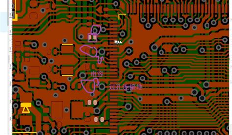
A. Design Rules and Constraints
Modern PCB design software (e.g., Altium Designer, KiCad, Cadence Allegro) allows designers to set Design Rule Checks (DRC) to enforce constraints such as:
- Trace width & spacing (based on current capacity and signal type)
- Via sizes (mechanical vs. laser microvias)
- Clearance rules (minimum distance between copper features)
- High-speed design rules (differential pairs, length matching)
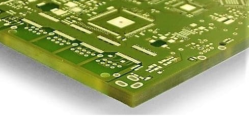
B. Layer Stackup Configuration
The PCB stackup defines the arrangement of conductive and insulating layers. Key considerations include:
- Number of layers (2-layer, 4-layer, or multilayer PCBs)
- Material selection (FR-4, Rogers, flex materials)
- Impedance control (critical for high-speed signals)
- Power and ground plane distribution (to reduce noise)
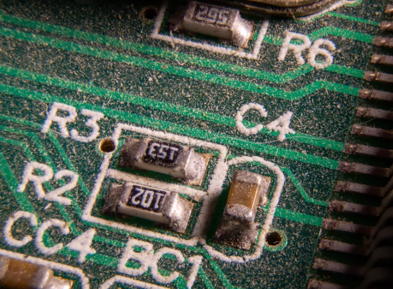
C. Component Placement and Routing Strategies
- Footprint selection (ensures components fit correctly)
- Thermal management (placement of heat-generating components)
- Routing priority (high-speed traces first, followed by power and ground)
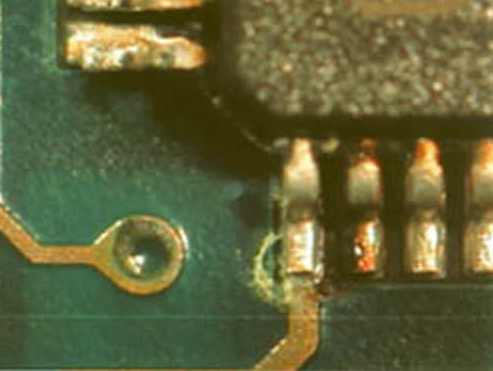
D. Manufacturing and Assembly Settings
- Gerber file settings (copper layers, solder mask, silkscreen)
- Drill files (specifying hole sizes and locations)
- Solder paste stencil design (for SMD components)
- Test point placement (for in-circuit testing)
4. Steps to Configure a PCB Project
Step 1: Define Project Requirements
- Determine the PCB’s purpose (digital, analog, RF, mixed-signal).
- Identify key constraints (size, operating environment, power requirements).
Step 2: Set Up Design Rules
- Configure trace widths based on current requirements.
- Define clearance rules for high-voltage sections.
- Set up differential pair routing for high-speed signals.
Step 3: Configure Layer Stackup
- Select the number of layers.
- Assign signal, power, and ground planes.
- Specify dielectric materials and thickness.
Step 4: Component Placement and Routing
- Place critical components (MCUs, connectors, power regulators) first.
- Route high-speed signals with controlled impedance.
- Ensure proper grounding and power distribution.
Step 5: Verify with DRC and ERC
- Run Design Rule Check (DRC) to detect violations.
- Perform Electrical Rule Check (ERC) to ensure schematic correctness.
Step 6: Generate Manufacturing Files
- Export Gerber files, drill files, and assembly drawings.
- Verify with the manufacturer to ensure compatibility.
5. Common Mistakes in PCB Configuration
- Ignoring DFM guidelines → Leads to fabrication issues.
- Incorrect impedance calculations → Causes signal integrity problems.
- Overlooking thermal management → Results in overheating.
- Poor layer stackup planning → Increases EMI and reduces performance.
6. Best Practices for Effective PCB Configuration
✔ Start with a template (reuse proven configurations).
✔ Collaborate with manufacturers early (avoid last-minute changes).
✔ Use simulation tools (verify signal and power integrity).
✔ Document all settings (for future revisions and team reference).
7. Conclusion
Configuring a PCB project is a foundational step that impacts the entire design process. By properly defining design rules, layer stackups, and manufacturing constraints, engineers can ensure a functional, reliable, and producible PCB. Neglecting configuration can lead to costly errors, whereas a well-structured setup streamlines development and improves product quality.
As PCB technology evolves (with HDI, flex PCBs, and high-speed designs), proper configuration becomes even more critical. By following best practices and leveraging modern design tools, engineers can optimize their PCB projects for performance and manufacturability.