What does pcb assembly mean
Understanding PCB Assembly: A Comprehensive Guide
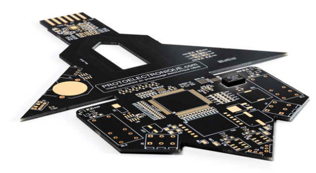
Printed Circuit Board (PCB) assembly is a critical process in the manufacturing of electronic devices, serving as the backbone for the functionality of modern electronics. To understand PCB assembly, it is essential to first grasp what a PCB is. A PCB is a flat board made of non-conductive material, typically fiberglass, that supports and connects various electronic components using conductive pathways, tracks, or signal traces etched from copper sheets laminated onto a non-conductive substrate. The assembly process involves several intricate steps that transform a bare PCB into a fully functional electronic circuit.
The initial phase of PCB assembly begins with the application of solder paste.
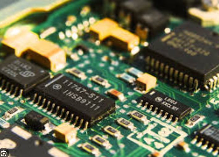
Solder paste, a mixture of tiny solder balls and flux, is applied to the PCB’s surface using a stencil. This paste is crucial as it temporarily holds the components in place and provides the necessary electrical connections once melted. Following the application of solder paste, the next step involves placing the electronic components onto the PCB. This is typically done using automated machines known as pick-and-place machines, which accurately position components such as resistors, capacitors, and integrated circuits onto the board.
Once the components are in place, the assembly process moves to the soldering stage.
There are two primary methods of soldering: reflow soldering and wave soldering. Reflow soldering is commonly used for surface-mount technology (SMT) components. In this method, the PCB with the placed components is passed through a reflow oven, where the solder paste is heated to its melting point, creating a permanent bond between the components and the PCB. On the other hand, wave soldering is used for through-hole components. In this process, the PCB is passed over a wave of molten solder, which adheres to the exposed metal areas and component leads, forming secure connections.
After soldering, the assembled PCB undergoes inspection and testing to ensure its functionality and reliability.
Automated optical inspection (AOI) systems are employed to check for common defects such as solder bridges, missing components, and misalignments. Additionally, X-ray inspection may be used to examine hidden solder joints, particularly in complex assemblies. Functional testing is also conducted to verify that the PCB performs as intended in its final application. This may involve in-circuit testing (ICT) or functional testing, where the PCB is subjected to electrical signals and monitored for correct responses.
The final steps in PCB assembly include cleaning and conformal coating.
Cleaning removes any residual flux and contaminants that could affect the performance and longevity of the PCB. Conformal coating involves applying a protective layer over the assembled PCB to shield it from environmental factors such as moisture, dust, and chemicals, thereby enhancing its durability.
In conclusion, PCB assembly is a multifaceted process that transforms a simple board into a sophisticated electronic circuit. It involves precise application of solder paste, accurate placement of components, effective soldering techniques, and rigorous inspection and testing. Each step is crucial in ensuring the reliability and functionality of the final product. As technology continues to advance, the methods and tools used in PCB assembly are also evolving, leading to more efficient and higher-quality electronic devices. Understanding the intricacies of PCB assembly provides valuable insight into the complex world of electronics manufacturing.
The Importance Of PCB Assembly In Modern Electronics
Printed Circuit Board (PCB) assembly is a critical process in the manufacturing of modern electronic devices. It involves the mounting of electronic components onto a PCB, which serves as the foundation for the electronic circuitry. This process is essential for the functionality and reliability of electronic products, ranging from simple gadgets to complex systems used in various industries. Understanding the importance of PCB assembly in modern electronics requires an appreciation of its role in ensuring the performance, durability, and efficiency of electronic devices.
To begin with, PCB assembly is fundamental to the miniaturization of electronic devices.
As technology advances, there is a growing demand for smaller, more compact devices that can perform multiple functions. PCB assembly techniques, such as Surface Mount Technology (SMT) and Through-Hole Technology (THT), enable the placement of numerous components in a limited space, thereby facilitating the creation of compact and efficient electronic products. This miniaturization is particularly crucial in consumer electronics, medical devices, and aerospace applications, where space constraints are a significant consideration.
Moreover, the reliability of electronic devices is heavily dependent on the quality of PCB assembly.
A well-assembled PCB ensures that all components are securely attached and properly connected, reducing the risk of malfunctions and failures. This reliability is vital in critical applications, such as medical equipment and automotive systems, where any failure could have severe consequences. High-quality PCB assembly processes, including precise soldering and thorough inspection, help to ensure that electronic devices operate consistently and safely over their intended lifespan.
In addition to reliability, PCB assembly also plays a crucial role in the performance of electronic devices.
The arrangement and connection of components on a PCB can significantly impact the electrical characteristics of the circuit, such as signal integrity and electromagnetic compatibility. Proper PCB assembly techniques help to optimize these characteristics, ensuring that the device performs as intended. For instance, careful placement of components and routing of traces can minimize signal interference and improve the overall efficiency of the circuit. This optimization is essential in high-performance applications, such as telecommunications and computing, where even minor deviations can affect the functionality of the device.
Furthermore, PCB assembly contributes to the cost-effectiveness of electronic manufacturing.
Automated assembly processes, such as pick-and-place machines and reflow soldering, enable the mass production of PCBs with high precision and consistency. This automation reduces labor costs and minimizes the likelihood of human error, leading to more efficient production and lower overall costs. Additionally, the use of standardized components and assembly techniques allows for economies of scale, further driving down the cost of electronic devices. This cost-effectiveness is particularly important in the consumer electronics market, where competitive pricing is a key factor in product success.
Lastly, the environmental impact of electronic manufacturing is an increasingly important consideration.
PCB assembly processes that prioritize sustainability, such as the use of lead-free solder and recyclable materials, help to reduce the environmental footprint of electronic devices. By adopting eco-friendly practices, manufacturers can contribute to the global effort to minimize electronic waste and promote sustainable development.
In conclusion, PCB assembly is a vital aspect of modern electronics, influencing the miniaturization, reliability, performance, cost-effectiveness, and environmental impact of electronic devices. As technology continues to evolve, the importance of high-quality PCB assembly will only grow, underscoring its significance in the development and production of innovative electronic products.
Key Steps In The PCB Assembly Process
Printed Circuit Board (PCB) assembly is a critical process in the manufacturing of electronic devices, involving the integration of electronic components onto a PCB to create a functional circuit. This process is essential for the production of a wide range of electronic products, from simple gadgets to complex machinery. Understanding the key steps in the PCB assembly process is crucial for anyone involved in electronics manufacturing or design.
The first step in the PCB assembly process is the design and fabrication of the PCB itself.
This involves creating a detailed layout of the circuit, which includes the placement of components and the routing of electrical connections. Once the design is finalized, the PCB is fabricated using materials such as fiberglass or composite epoxy. The board is then coated with a layer of copper, which is etched away to create the desired circuit pattern.
Following the fabrication of the PCB, the next step is the application of solder paste.
Solder paste is a mixture of tiny solder balls and flux, which helps to clean the surfaces and improve the flow of solder. The paste is applied to the PCB using a stencil, which ensures that it is deposited only on the areas where components will be placed. This step is critical for ensuring that the components are securely attached to the board.
Once the solder paste has been applied, the components are placed onto the PCB.
This is typically done using automated machines known as pick-and-place machines, which can accurately position components at high speeds. These machines use a combination of vacuum and mechanical grippers to pick up components from a reel or tray and place them onto the board. The accuracy and speed of these machines are essential for maintaining the efficiency and quality of the assembly process.
After the components have been placed, the next step is the reflow soldering process.
During reflow soldering, the PCB is passed through a reflow oven, which heats the board to a temperature that melts the solder paste. This causes the solder to flow and form a strong bond between the components and the PCB. The board is then gradually cooled, solidifying the solder and securing the components in place. This step is crucial for ensuring the electrical and mechanical integrity of the assembled PCB.
Following reflow soldering, the assembled PCB undergoes inspection and testing to ensure that it meets the required specifications.
This can include visual inspection, automated optical inspection (AOI), and X-ray inspection to check for defects such as solder bridges, missing components, or misalignments. Electrical testing is also performed to verify that the circuit functions correctly. This can involve in-circuit testing (ICT), which checks the electrical connections and component values, as well as functional testing, which simulates the operating conditions of the final product.
Finally, any necessary post-assembly processes are carried out, such as cleaning the PCB to remove any residual flux or contaminants.
The board may also undergo conformal coating, which involves applying a protective layer to shield the components from environmental factors such as moisture and dust. Once these steps are completed, the assembled PCB is ready for integration into the final product.
In conclusion, the PCB assembly process involves several key steps, each of which is critical for ensuring the quality and functionality of the final product. From the initial design and fabrication of the PCB to the placement of components and reflow soldering, each stage requires precision and attention to detail. By understanding these steps, manufacturers can produce reliable and high-quality electronic devices that meet the demands of today’s technology-driven world.
Common Challenges And Solutions In PCB Assembly
Printed Circuit Board (PCB) assembly is a critical process in the manufacturing of electronic devices, involving the mounting of electronic components onto a PCB to create a functional circuit. Despite its importance, PCB assembly is fraught with numerous challenges that can impact the quality, reliability, and performance of the final product. Understanding these common challenges and their solutions is essential for ensuring successful PCB assembly.
One of the primary challenges in PCB assembly is component placement accuracy.
As electronic devices become more compact and complex, the need for precise placement of components on the PCB becomes increasingly critical. Misalignment or incorrect placement can lead to short circuits, signal integrity issues, and overall device malfunction. To address this, advanced pick-and-place machines equipped with high-resolution cameras and sophisticated algorithms are employed. These machines ensure that components are placed with pinpoint accuracy, minimizing the risk of errors.
Another significant challenge is soldering defects, which can manifest as solder bridges, cold joints, or insufficient solder.
These defects can compromise the electrical connections between components and the PCB, leading to intermittent or complete failure of the device. Implementing stringent process controls and using high-quality soldering materials can mitigate these issues. Additionally, automated optical inspection (AOI) systems can be used to detect soldering defects early in the assembly process, allowing for timely corrective actions.
Thermal management is also a critical concern in PCB assembly, particularly for high-power applications.
Inadequate thermal management can result in overheating, which can damage components and reduce the lifespan of the device. To address this, designers often incorporate thermal vias, heat sinks, and thermal pads into the PCB layout. Moreover, selecting components with appropriate thermal ratings and using thermal interface materials can further enhance heat dissipation.
Electrostatic discharge (ESD) is another challenge that can adversely affect PCB assembly.
ESD can damage sensitive electronic components, leading to latent defects that may not be immediately apparent but can cause failures over time. To mitigate ESD risks, assembly facilities implement ESD control measures such as grounding wrist straps, ESD-safe workstations, and ionizing air blowers. Additionally, handling components with care and using ESD-safe packaging materials can further reduce the risk of ESD damage.
Component availability and supply chain issues can also pose significant challenges in PCB assembly.
Shortages of critical components can delay production schedules and increase costs. To address this, manufacturers often establish strong relationships with multiple suppliers and maintain a buffer stock of essential components. Additionally, designing PCBs with alternative component options can provide flexibility in case of supply chain disruptions.
Finally, ensuring compliance with industry standards and regulations is crucial in PCB assembly.
Non-compliance can result in product recalls, legal issues, and damage to the manufacturer’s reputation. Adhering to standards such as IPC-A-610 for assembly workmanship and IPC-6012 for PCB fabrication ensures that the assembled PCBs meet the required quality and reliability criteria. Regular audits and inspections can help maintain compliance and identify areas for improvement.
In conclusion, PCB assembly is a complex process that involves numerous challenges, from component placement accuracy to thermal management and ESD protection. By employing advanced technologies, implementing stringent process controls, and adhering to industry standards, manufacturers can overcome these challenges and ensure the production of high-quality, reliable electronic devices. Understanding and addressing these common challenges is essential for the success of any PCB assembly operation.


