What does PCB tombstoning mean? How can you prevent it?
Today’s article will focus on: PCB tombstoning, PCB tombstoning analysis, prevention, and solutions.
I.What is PCB tombstoning?
Tombstoning typically affects surface-mount passive components such as resistors, capacitors, and inductors. During the soldering process, one end of the component lifts off the PCB pad.
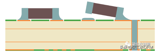
PCB tombstoning: The final angle of a component can range from a few degrees to 90 degrees. Regardless of the angle, the end result is that one of the component terminals is not soldered to the PCB pad, creating an open circuit.
II.PCB tombstoning analysis
Tombstoning occurs when one end of an MLCC (Multi-layer Copper CC) leaves the soldering area during soldering, tilting or lifting. This is primarily due to unbalanced wetting between the two ends of the MLCC during soldering. The main factors that cause unbalanced wetting forces are: 1. MLCC ends cannot be melted simultaneously. 2. Improper pad design. Based on mechanical mechanisms, it is recommended to keep the MLCC surface clean and ensure proper pad design to prevent loss of solder paste activity and ensure melting of both ends. This measure effectively prevents tombstoning and has demonstrated good results in actual production. Before soldering, the ends of a multilayer ceramic capacitor (MLCC) are temporarily positioned using solder paste and a pad. Once soldering is successfully completed, they become part of the assembled circuit board. If the ends are unevenly wetting during soldering, the uneven surface tension generated can cause one end to slide off the substrate, or the entire MLCC to warp or even stand upright. This phenomenon, resembling a standing tomb, is commonly known as tombstoning, sometimes also called the drawbridge phenomenon. This phenomenon directly impacts the quality and reliability of printed circuit boards and entire devices. It also increases the manufacturer’s return rate and costs.
III. Causes and Solutions for PCB Tombstoning
Trace Pad Issues
PTH Close to Pad
Pad Connected to Large Copper Area
Via-in-Pad
Pad Shape and Position
Legend Under Component
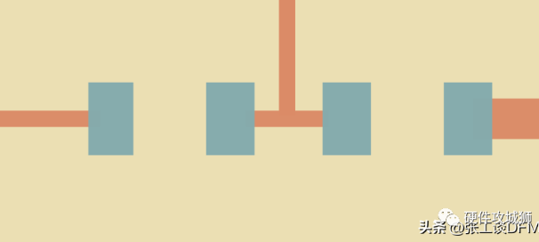
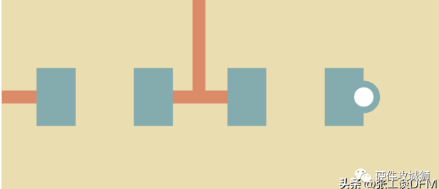
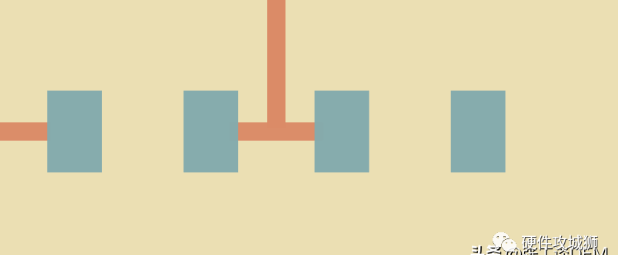
- Trace Pad Issues Symptom: Pads connected to multiple traces dissipate heat faster than pads connected to a single trace. However, the wetting process will complete at different times, potentially leading to tombstoning. Avoid having multiple traces on one pad and only one trace on another. Avoid having different trace widths on the same component pads. Figure 1 below shows a common layout, and Figure 2 shows a recommended layout.

General Layout

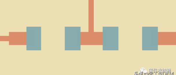
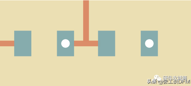
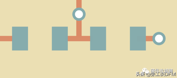
Recommended Alternative Layout: When pads are connected to power or GND, using larger traces, as shown in the figure below, is common. However, this can cause the pads with larger traces to wet before the pads with thinner traces, potentially leading to tombstoning.
Pads Connected to Power or GND: Solution: Two solutions are shown below to achieve the same trace width for each component pad. An important consideration is that this uniform trace width must be at least 0.25mm from the pad edge before the width changes to help synchronize the wetting process.

- Plated Through Holes (PTHs) Too Close to Pads: Symptom: Any plated through hole (PTH), including vias, with pads too close to the component pad will dissipate heat more quickly during wetting. The edge of the component pad should be at least 0.25mm away from the edge of the actual hole. Furthermore, if the PTH is too close to the component pad to ensure a reliable solder mask, solder can flow into the hole (known as non-wicking or solder overflow). The following image shows a layout where the PTH is too close to the component pad:

Layout where the PTH is too close to the component pad. The image below shows that the minimum distance from the edge of the PTH pad to the edge of the hole is 0.25mm.
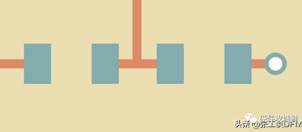
The minimum distance from the edge of the PTH pad to the edge of the hole is 0.25mm. Solution 1) Using a via in pad can help reduce the copper area of the pad, but the via in pad process itself will dissipate heat.
Use via-in-pad. 2) A more reliable solution is to move the via at least 0.25mm from the edge of the component pad to the edge of the via.

Move the via at least 0.25mm from the edge of the component pad to the edge of the via. 3. Pads connected to large copper areas. Symptom: Large copper areas act as heat sinks, but connecting component pads to one another can cause a tombstoning effect, as shown in the figure below.

Connecting to pads on large copper areas

Connecting to pads on large copper areas: Solution: Ensure similarly sized traces are connected to two pads, as shown in the image below. Additionally, allow at least 0.25mm of trace clearance before the copper area.

Ensure similarly sized traces are connected to two pads. If high power is involved, use a similar solution to the above (trace pad issue). 4. Via-in-Pad: Symptom: With the increasing miniaturization of electronic products, vias are often used in component pads. However, wicking and escaping along the pads can lead to uneven wetting. Even if both component pads have vias, there’s a significant chance that one will complete wetting before the other, depending on what the via is connected to, and tombstoning can still occur. Furthermore, with vias in pads, there’s the issue of sufficient solder paste to fill the via and still adhere to the component terminal during reflow. The image below shows a via in a component pad. Because the via is unfilled, solder paste can wick and escaping into the hole, potentially causing tombstoning or desoldering of the component terminal.
Via in Component Pad: Solution 1: Via Fill. Via filling is a solution that helps reduce the risk of tombstoning.
Via Fill 2. Moving the via at least 0.25mm from the edge of the component pad to the edge of the via is a more reliable solution.
Moving the via at least 0.25mm from the edge of the component pad to the edge of the via. 5. Pad Shape and Position Symptom: If the pad size is too large, it can cause component shifting or rotation, or tombstoning. If the pad position deviates too much from the required position for that specific component, the soldering process will likely yield poor results. Solution: Use IPC standard pad shapes and sizes to avoid these issues. Compare the pads in your CAD system to those recommended in the IPC standards. 6. Component Legend Symptom: Inappropriate legends can cause tombstoning even on smaller components. The copper layer, solder mask, and legend layer together can create points that are much taller than the copper pad height. See resistor R2 in the image below.
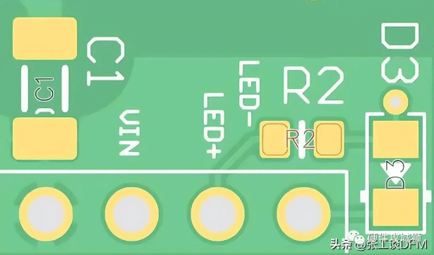
Component pads have traces between them, with solder mask and legends above them.
Solution: This is particularly important for small components (such as 0603); avoid placing the legend underneath these components.
IV. Measures to Prevent PCB Tombstoning
- Solder Both Ends Simultaneously: Solder as quickly as possible to minimize the difference in melting between the two ends. Avoid soldering one end while the other is still unmelted (see Figure 1). This will likely be pulled up by the surface tension and soldering force of the other end (see Figure 2 below).
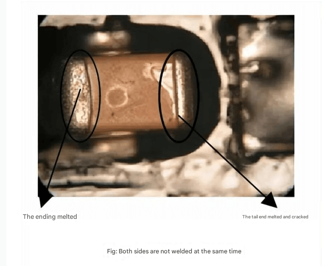
Uneven melting at both ends
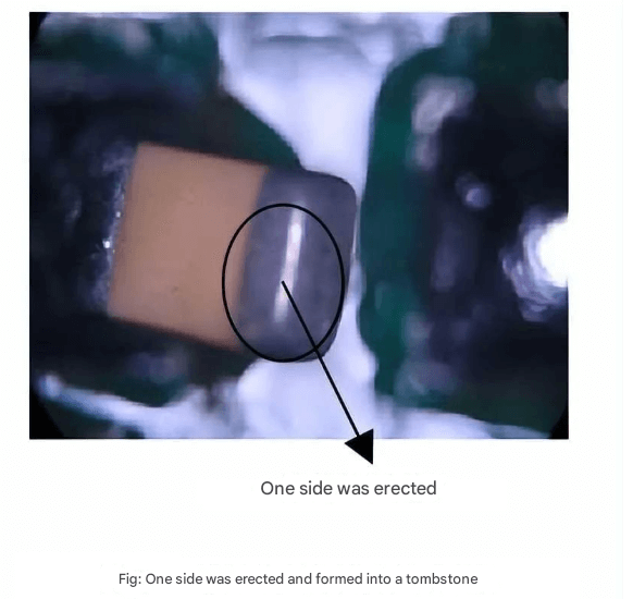
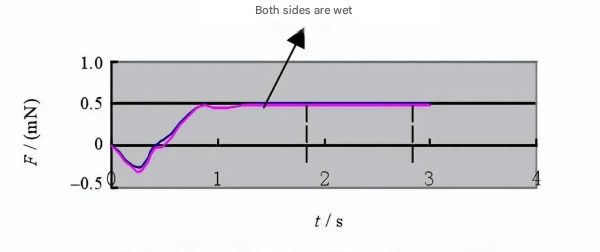
Tombstone phenomenon 2. Proper pad design: A pair of MLCC pads of different sizes or asymmetry will result in inconsistent solder paste application. The smaller pad reacts quickly to temperature, melting the solder paste on it easily. The opposite is true for the larger pad. As the solder paste melts on the smaller pad, the MLCC is stretched straight by the surface tension of the solder paste, causing tombstone phenomenon. Therefore, the following aspects should be considered in the design: 1) The solder joint should be as wide as possible, with at least 0.3mm overlap between the MLCC metal end and the pad. 2) The pad space should be kept as short as possible, sufficient to fill with solder. Generally, the remaining length should not exceed 0.5mm. If the chamber must be extended to accommodate test probes, consider the shrinkage of the printed surface in advance. 3) The width of the pad itself should not be too wide; compared to MLCC, the ideal width should not exceed 0.25mm. 3. Maintaining Solder Paste Activity: Solder paste is a relatively sensitive soldering material. Contamination, oxidation, or moisture absorption can all cause varying degrees of degradation. Deterioration of the solder paste can affect printing results and, more seriously, cause solder defects such as the tombstoning effect. Therefore, the following points should be observed during processing: 1) Solder paste should be stored in an environment of 5-10°C. 2) Do not open solder paste immediately after removing it from the refrigerator to prevent moisture from condensing into the paste. Generally, it should be used after it reaches room temperature. 3) Thoroughly stir the solder paste before use. 4) Unused solder paste remaining in the tank should be covered with inner and outer covers and not exposed to air to prevent moisture absorption and oxidation. 5) After the job is completed, transfer any remaining solder on the stencil to an empty container for future use. Used solder paste should not be poured back into unused solder paste, as this will contaminate the paste and deteriorate the fresh solder paste. 6) The solder paste printing process should be performed away from frequently opened windows and doors to maintain a stable operating temperature and prevent local environmental fluctuations caused by outside air. 4. Implement anti-contamination measures. If the MLCC surface is contaminated, it will lead to poor wetting and cause tombstoning. Therefore, both MLCC manufacturers and users need to implement anti-contamination measures. The figure below shows typical wetting curves for MLCCs with and without contamination on one end face.
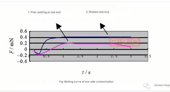
Wetting curve for a contaminated end face