What File Type is Used for PCB Designs?
Introduction to PCB Design Files
Printed Circuit Board (PCB) design is a complex process that involves multiple stages from conceptualization to manufacturing. Throughout this process, various file types are used to capture different aspects of the design. These files serve as the digital blueprints that contain all the necessary information about the PCB’s layout, components, connections, and manufacturing specifications.
Understanding PCB file types is crucial for designers, engineers, and manufacturers as they facilitate collaboration, ensure design integrity, and enable seamless transition between different stages of PCB development. The electronics industry has developed several standardized file formats that allow PCB designs to be shared across different software tools and manufacturing processes.
This article explores the most common file types used in PCB design, their purposes, and how they contribute to the overall PCB development workflow. We’ll examine schematic files, layout files, manufacturing outputs, and other specialized formats that make modern PCB design possible.
Schematic Capture Files
The PCB design process typically begins with schematic capture, where the electrical connections between components are defined. Several file formats are used at this stage:
1. SCH Files
SCH files are the native schematic files used by many EDA (Electronic Design Automation) tools. These binary files contain all the information about the schematic diagram, including components, their properties, and how they’re connected. Different EDA tools use their own proprietary SCH formats, which are generally not interchangeable between software packages.
2. DSL (Design System Language) Files
Some advanced EDA tools use DSL files that describe the schematic in a text-based format. These files are human-readable and can sometimes be modified outside of the EDA software, though this requires specialized knowledge.
3. XML-based Schematic Formats
Modern EDA tools are increasingly adopting XML-based formats for schematic storage. These offer better interoperability and are easier to parse programmatically. Examples include the KiCad schematic format (.kicad_sch) which uses an XML structure.
PCB Layout Files
Once the schematic is complete, the design moves to the PCB layout stage where the physical board is designed. The primary file types used include:
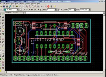
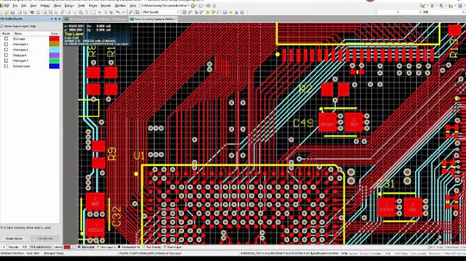
1. BRD Files
BRD files are the native board layout files used by many PCB design tools. Like SCH files, these are typically proprietary binary formats that contain all the information about the PCB layout, including component placement, copper traces, vias, and board outline. Popular EDA tools like Cadence Allegro and Eagle use BRD files.
2. PCB Files
Some tools use the .pcb extension for their native layout files. These are functionally similar to BRD files but follow different internal structures depending on the software that created them.
3. KiCad PCB Files (.kicad_pcb)
KiCad uses an XML-based format for its PCB layouts, making them more transparent and easier to work with using external tools. The .kicad_pcb file contains all the information about the board’s layers, footprints, tracks, and other design elements.
Intermediate Exchange Formats
To enable collaboration between different EDA tools and between designers and manufacturers, several intermediate file formats have been developed:
1. Gerber Files (RS-274X)
Gerber files are the industry standard for PCB manufacturing data transfer. The modern Gerber format (RS-274X) is used to describe each layer of the PCB as a 2D vector image. A complete PCB design typically consists of multiple Gerber files:
- Top copper layer (.GTL)
- Bottom copper layer (.GBL)
- Inner copper layers (.G1, .G2, etc.)
- Solder mask layers (.GTS, .GBS)
- Silkscreen layers (.GTO, .GBO)
- Drill drawing (.GDD)
- Board outline (.GKO or .GM1)
Gerber files are essentially photoplotter instructions that tell PCB manufacturers how to image each layer of the board.
2. Excellon Drill Files
Excellon format files (typically with .TXT or .DRL extensions) contain information about all the holes that need to be drilled in the PCB, including their locations, sizes, and whether they’re plated or non-plated. These files work in conjunction with Gerber files to provide complete manufacturing instructions.
3. ODB++
ODB++ is a more comprehensive alternative to Gerber/Excellon that packages all PCB manufacturing data into a single, intelligent database. Developed by Valor (now part of Siemens), ODB++ includes not just the graphical data but also the netlist, materials, and stackup information in a structured directory format.
4. IPC-2581
IPC-2581 is an emerging open standard for PCB design data exchange that aims to replace both Gerber and ODB++. It provides a complete, unambiguous description of the PCB in a single XML file, including schematic, layout, and manufacturing information.
Netlist Files
Netlists describe the electrical connectivity of the PCB design and are used for verification and simulation:
1. SPICE Netlists (.CIR)
Used for circuit simulation, SPICE netlists describe components and their connections in a text format that can be processed by simulation tools like LTspice or NGspice.
2. EDIF (Electronic Design Interchange Format)
EDIF is a vendor-neutral format used to exchange netlist and schematic information between different EDA tools. It’s particularly useful when moving designs between schematic capture and PCB layout tools from different vendors.
3. Verilog Netlists
Used primarily in digital design, Verilog netlists describe the design at the gate level and are often used for FPGA and ASIC design as well as PCB verification.
3D Model Files
Modern PCB design often incorporates 3D visualization and mechanical integration:
1. STEP Files (.STP, .STEP)
STEP (Standard for the Exchange of Product Data) files are the most common format for exchanging 3D PCB models with mechanical CAD tools. They accurately represent the board and components in three dimensions.
2. VRML Files (.WRL)
VRML (Virtual Reality Modeling Language) files are sometimes used for simpler 3D representations of PCBs, particularly in web-based viewers.
3. IDF Files
IDF (Intermediate Data Format) files are used specifically for exchanging PCB and component geometry between ECAD and MCAD systems. They contain both board outline and component placement information.
Manufacturing Output Files
Additional files are generated to support the manufacturing process:
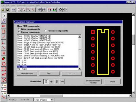
1. Bill of Materials (BOM) Files
BOMs list all components needed to assemble the PCB. These are typically in CSV, Excel (.XLSX), or XML format and include part numbers, quantities, descriptions, and reference designators.
2. Pick and Place Files
These machine-readable files (usually CSV or TXT) provide coordinates and orientations for all components on the PCB, used by automated assembly machines.
3. Test Point Files
Files containing test point locations and net associations, used for manufacturing test fixture development.
Proprietary vs. Open Formats
The PCB industry uses both proprietary and open file formats:
1. Proprietary Formats
Most major EDA tools use proprietary formats for their native design files (like .BRD, .SCH). These offer complete representation of the design within that tool but can create interoperability challenges.
2. Open Standards
Formats like Gerber, ODB++, and IPC-2581 are open standards that facilitate collaboration across different tools and between designers and manufacturers.
Choosing the Right File Types
The selection of file types depends on several factors:
- Design Stage: Schematic vs. layout vs. manufacturing
- Tool Compatibility: What software is being used in the workflow
- Collaboration Needs: Whether files need to be shared with others
- Manufacturing Requirements: What formats your PCB fabricator accepts
For most professional workflows, a combination of native formats for design and open standards for manufacturing is typical.
Future Trends in PCB File Formats
The PCB industry is moving toward more intelligent, integrated file formats:
- Increased Adoption of IPC-2581: As more tools support it, this comprehensive format may replace Gerber for manufacturing.
- Cloud-Based Design: Some tools are moving to web-native formats that enable real-time collaboration.
- Increased Standardization: Efforts continue to reduce the number of proprietary formats in favor of open standards.
- Enhanced 3D Integration: Formats that better combine electrical and mechanical design data are emerging.
Conclusion
PCB design involves a complex ecosystem of file types, each serving specific purposes in the design and manufacturing workflow. From schematic capture (SCH files) to board layout (BRD files) to manufacturing outputs (Gerber, Excellon), these files collectively contain all the information needed to transform an electronic concept into a physical circuit board.
Understanding these file types is essential for effective PCB design collaboration and manufacturing. While proprietary formats offer rich functionality within specific tools, open standards like Gerber and IPC-2581 ensure that designs can be reliably manufactured regardless of the EDA software used.
As the industry evolves, we can expect continued progress toward more integrated, intelligent file formats that streamline the entire PCB development process while maintaining compatibility across the diverse ecosystem of design tools and manufacturing systems.