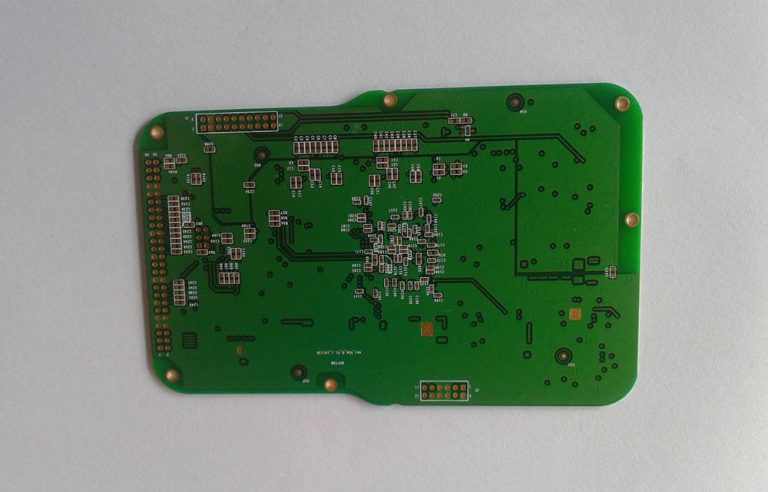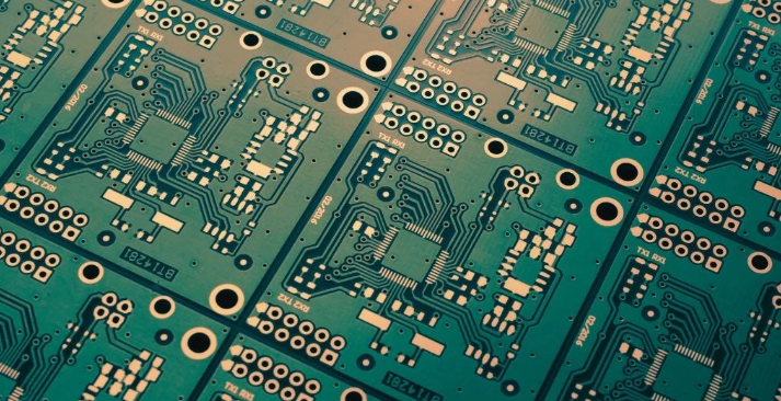
What information does the Rogers PCB picture have?
1. The number of layers:
A picture can show the number of layers in the PCB, which can range from single-layer to multi-layer boards.
2. Copper traces:
The picture can show the copper traces that connect the components on the board.
3. Solder mask:
The picture can show the solder mask, which is a protective layer that covers the copper traces and prevents them from oxidizing.
4. Silkscreen:
The picture can show the silkscreen, which is the labeling on the board that identifies the components and their locations.
5. Thickness:
The picture can give an idea of the thickness of the board, which can vary depending on the application.
6. Material:
The picture can also reveal the material used for the PCB, which in this case is Rogers, a high-frequency substrate material known for its excellent electrical properties.
Overall, a picture of a Rogers PCB can provide valuable information about the board’s design, construction, and functionality.

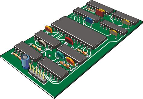
The role of Rogers PCB pictures
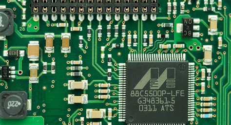
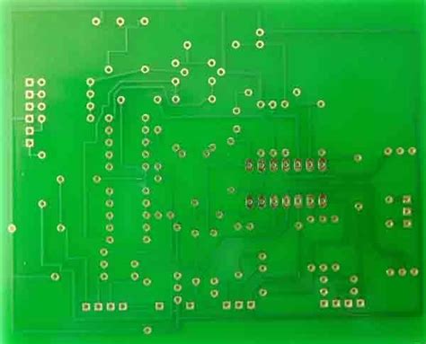
Rogers PCB pictures play a crucial role in the design and manufacturing process of Rogers PCBs. These pictures provide a visual representation of the PCB layout, including the placement of components, traces, and vias.
They allow designers and manufacturers to verify the accuracy of the design and identify any potential issues before the PCB is fabricated.
Rogers PCB pictures also help in the assembly process by providing a reference for the placement and orientation of components.
They can also be used for troubleshooting and repair purposes, as they provide a clear view of the PCB layout and any potential faults.
Overall, Rogers PCB pictures are an essential tool for ensuring the quality and accuracy of Rogers PCB designs and manufacturing processes.

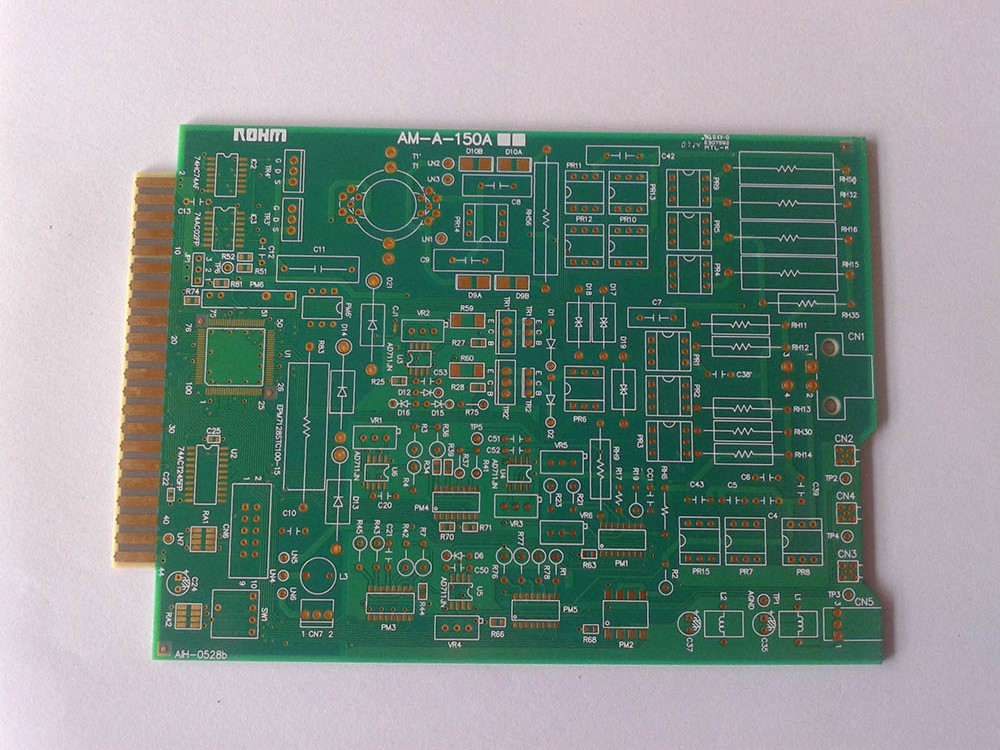
Pathway to Rogers PCB Image
The pathway to obtain a Rogers PCB image may vary depending on the specific design and manufacturing process being used.
However, here are some general steps that may be involved:
1. Design the PCB layout using a software tool such as Altium, Eagle, or KiCad. This software will generate a digital image of the PCB layout.
2. Verify the design using a design rule check (DRC) tool to ensure that the layout meets the required specifications.
3. Generate a Gerber file, which is a standard format used for manufacturing PCBs. This file contains the information needed to create the physical PCB, including the copper traces, pads, and drill holes.
4. Send the Gerber file to the PCB manufacturer, along with any additional instructions or specifications.

5. The manufacturer will use the Gerber file to create the physical PCB, which will include the Rogers substrate material.
6. Once the PCB is fabricated, it can be inspected and tested to ensure that it meets the required specifications.
7. A Rogers PCB image can be obtained by taking a photograph or scanning the physical PCB. This image can be used for documentation, troubleshooting, or other purposes.