What Is a Memory Module PCB?
Introduction
Memory modules are essential components in modern computing systems, enabling data storage and retrieval for processors. At the heart of every memory module lies the Printed Circuit Board (PCB), which serves as the foundation for mounting memory chips and facilitating electrical connections. This article explores the structure, design, materials, and manufacturing processes of memory module PCBs, as well as their role in memory performance and reliability.
1. The Basics of Memory Module PCBs
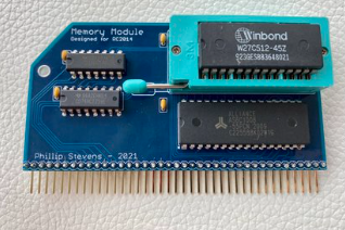
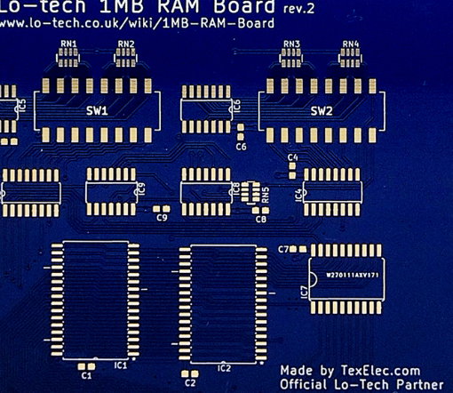
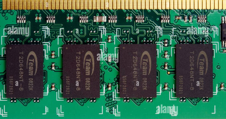
A memory module PCB is a specialized circuit board designed to hold Dynamic Random-Access Memory (DRAM) chips and provide electrical pathways for data transfer between the memory and the computer’s motherboard. Common types of memory modules include:
- DIMM (Dual In-line Memory Module) – Used in desktops and servers.
- SO-DIMM (Small Outline DIMM) – Used in laptops and compact systems.
- UDIMM, RDIMM, LRDIMM – Variations with different buffering and rank configurations.
The PCB ensures signal integrity, power distribution, and mechanical stability for the memory chips.
1.1 Layers and Structure
Memory module PCBs are typically multilayer boards, ranging from 4 to 10 layers, depending on the memory type and speed requirements. Key layers include:
- Signal Layers – Carry data and control signals between DRAM chips and the memory controller.
- Power Planes – Distribute stable voltage to memory chips.
- Ground Planes – Reduce electromagnetic interference (EMI) and provide return paths for signals.
1.2 Key Components on the PCB
- DRAM Chips – The primary memory ICs (e.g., DDR4, DDR5 chips).
- SPD (Serial Presence Detect) Chip – Stores memory configuration data.
- Resistors & Capacitors – Ensure signal integrity and power stability.
- Gold or Tin Fingers (Edge Connectors) – Interface with the motherboard’s memory slot.
2. PCB Design Considerations for Memory Modules
Designing a memory module PCB requires careful consideration of electrical, thermal, and mechanical factors.
2.1 Signal Integrity
- Impedance Control – High-speed memory (e.g., DDR5) requires precise trace impedance (typically 40–60 Ω) to prevent signal reflections.
- Trace Length Matching – Data lines must have matched lengths to avoid timing skew.
- Crosstalk Mitigation – Proper spacing and shielding reduce interference between signals.
2.2 Power Delivery
- Decoupling Capacitors – Stabilize voltage supply to DRAM chips.
- Low-Resistance Power Planes – Minimize voltage drops across the PCB.
2.3 Thermal Management
- Copper Pouring – Helps dissipate heat from DRAM chips.
- Thermal Vias – Improve heat transfer to inner layers or heat spreaders.
3. Materials Used in Memory Module PCBs
The choice of PCB materials affects performance, durability, and cost.
3.1 Substrate Materials
- FR-4 (Flame Retardant-4) – The most common material, offering good electrical insulation and mechanical strength.
- High-Tg FR-4 – Used for high-speed memory modules due to better thermal stability.
- Low-Loss Materials (e.g., Rogers, Isola) – Used in ultra-high-speed memory to reduce signal loss.
3.2 Copper Foil
- Electrodeposited (ED) Copper – Standard choice for most PCBs.
- Rolled Annealed Copper – Smoother surface, better for high-frequency signals.
3.3 Surface Finishes
- ENIG (Electroless Nickel Immersion Gold) – Provides excellent oxidation resistance.
- OSP (Organic Solderability Preservative) – Cost-effective but less durable.
4. Manufacturing Process of Memory Module PCBs
The production of memory module PCBs involves several key steps:
4.1 PCB Fabrication
- Lamination – Multiple layers of copper and dielectric material are pressed together.
- Drilling – Holes for vias and component mounting are drilled.
- Plating – Copper is deposited in drilled holes to create electrical connections.
- Etching – Unwanted copper is removed to form circuit traces.
- Solder Mask Application – A protective coating is applied to prevent short circuits.
- Silkscreen Printing – Labels and markings are added for assembly guidance.
4.2 Component Assembly
- SMT (Surface Mount Technology) – DRAM chips and passive components are placed using pick-and-place machines.
- Reflow Soldering – Components are permanently attached using high-temperature soldering.
- Testing & Inspection – Automated optical inspection (AOI) and electrical testing ensure quality.
5. The Role of PCB in Memory Performance
The PCB’s design and quality directly impact memory performance in several ways:
5.1 Speed and Bandwidth
- Higher Layer Counts Allow for better signal routing in high-speed DDR5 modules.
- Optimized Trace Layouts Reduce latency and improve data transfer rates.
5.2 Reliability
- Robust Power Delivery Prevents voltage fluctuations that can cause errors.
- Thermal Management Extends the lifespan of DRAM chips.
5.3 Overclocking Potential
- High-Quality PCBs With better materials and design allow for stable overclocking.
6. Future Trends in Memory Module PCBs
As memory technology evolves, PCB designs must adapt:
- Higher Speeds (DDR6 & Beyond) – Requires advanced materials and tighter impedance control.
- 3D Stacked Memory (HBM, HMC) – Demands specialized interposer PCBs.
- AI-Optimized Designs – Machine learning may optimize PCB layouts for performance.
Conclusion
The memory module PCB is a critical yet often overlooked component that ensures the proper functioning of DRAM in computing systems. Its design, materials, and manufacturing processes play a vital role in determining memory speed, stability, and longevity. As memory technology advances, PCBs will continue to evolve, enabling faster, more efficient, and more reliable memory solutions.
Understanding memory module PCBs helps engineers, enthusiasts, and manufacturers optimize performance and push the boundaries of modern computing.


