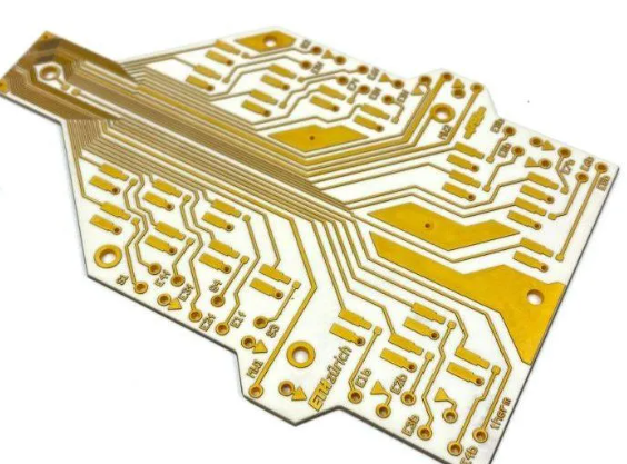
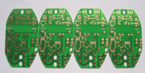
What is a pcb prototype
Understanding The Basics Of PCB Prototypes
A Printed Circuit Board (PCB) prototype is an essential component in the development and testing of electronic circuits. It serves as a preliminary version of a PCB, allowing engineers and designers to evaluate the functionality, performance, and reliability of their designs before mass production. Understanding the basics of PCB prototypes is crucial for anyone involved in electronics design and manufacturing, as it provides a foundation for creating efficient and effective electronic devices.
To begin with, a PCB prototype is typically created during the initial stages of product development.
It is used to test and validate the design, ensuring that all components are correctly placed and that the circuit functions as intended. This process involves several steps, starting with the design phase, where engineers use specialized software to create a schematic diagram of the circuit. This diagram is then converted into a layout, which specifies the physical arrangement of components and the routing of electrical connections on the board.
Once the design is complete, the next step is to fabricate the PCB prototype.
This involves transferring the layout onto a physical board, usually made of a non-conductive substrate such as fiberglass or epoxy. The board is then coated with a thin layer of conductive material, typically copper, which forms the electrical pathways. Advanced techniques such as photolithography and etching are used to create precise patterns on the board, ensuring that the electrical connections are accurate and reliable.
After fabrication, the PCB prototype undergoes a series of tests to verify its functionality.
These tests may include electrical testing, where engineers check for continuity and proper signal flow, as well as functional testing, where the prototype is integrated into a larger system to ensure it performs as expected. Any issues or defects identified during testing can be addressed through iterative design modifications, allowing for continuous improvement of the prototype.
The importance of PCB prototypes cannot be overstated, as they play a critical role in minimizing risks and reducing costs associated with product development.
By identifying and resolving design flaws early in the process, companies can avoid costly rework and delays in production. Moreover, PCB prototypes enable designers to experiment with different configurations and components, optimizing the performance and efficiency of the final product.
In addition to their role in testing and validation, PCB prototypes also facilitate communication and collaboration among team members.
Engineers, designers, and stakeholders can use the prototype as a tangible reference, discussing potential improvements and making informed decisions based on real-world data. This collaborative approach ensures that all aspects of the design are thoroughly considered, leading to a more robust and reliable final product.
Furthermore, advancements in technology have made PCB prototyping more accessible and efficient than ever before.
Rapid prototyping techniques, such as 3D printing and automated assembly, allow for quick turnaround times and reduced costs. These innovations enable companies to iterate rapidly, bringing new products to market faster and more efficiently.
In conclusion, understanding the basics of PCB prototypes is essential for anyone involved in electronics design and manufacturing. PCB prototypes serve as a crucial tool for testing and validating designs, minimizing risks, and optimizing performance. By leveraging advanced prototyping techniques and fostering collaboration among team members, companies can create high-quality electronic devices that meet the demands of today’s competitive market.
The Importance Of PCB Prototyping In Electronics Design
A PCB prototype, or Printed Circuit Board prototype, is an essential component in the electronics design process. It serves as a preliminary version of a circuit board, allowing engineers and designers to test and validate their designs before committing to full-scale production. The importance of PCB prototyping in electronics design cannot be overstated, as it plays a critical role in ensuring the functionality, reliability, and manufacturability of electronic devices.
To begin with, PCB prototyping allows for the early detection of design flaws.
By creating a prototype, designers can physically test their circuits and identify any issues that may not have been apparent during the initial design phase. This early detection is crucial because it enables designers to make necessary adjustments before mass production, thereby saving time and resources. Moreover, identifying and rectifying errors at the prototyping stage helps prevent costly recalls and redesigns later in the product development cycle.
In addition to error detection, PCB prototyping facilitates the optimization of circuit designs.
Prototyping provides an opportunity to experiment with different components, layouts, and configurations to achieve the best possible performance. This iterative process of testing and refining ensures that the final product meets the desired specifications and operates efficiently. Furthermore, prototyping allows designers to evaluate the thermal and electrical performance of their circuits, ensuring that they can withstand real-world operating conditions.
Another significant advantage of PCB prototyping is its role in verifying the manufacturability of a design.
A prototype serves as a tangible representation of the final product, enabling manufacturers to assess the feasibility of producing the circuit board at scale. This assessment includes evaluating the complexity of the design, the availability of components, and the compatibility with existing manufacturing processes. By addressing these factors during the prototyping phase, designers can make informed decisions that streamline the transition to mass production.
Moreover, PCB prototyping is instrumental in reducing development time.
By providing a platform for rapid testing and iteration, prototyping accelerates the design process and shortens the time-to-market for new products. This speed is particularly important in the fast-paced electronics industry, where staying ahead of the competition is crucial. Additionally, the ability to quickly produce and test prototypes allows for more frequent design reviews and feedback, fostering a collaborative environment that enhances the overall quality of the final product.
Furthermore, PCB prototyping supports innovation by enabling designers to explore new ideas and technologies.
Prototyping provides a low-risk environment for experimenting with novel concepts and pushing the boundaries of what is possible in electronics design. This freedom to innovate is essential for driving technological advancements and creating cutting-edge products that meet the evolving needs of consumers.
In conclusion, the importance of PCB prototyping in electronics design is multifaceted. It enables early detection of design flaws, facilitates optimization, verifies manufacturability, reduces development time, and supports innovation. By incorporating prototyping into the design process, engineers and designers can ensure that their products are functional, reliable, and ready for mass production. As the electronics industry continues to evolve, the role of PCB prototyping will remain a cornerstone of successful product development, driving progress and innovation in the field.
Steps Involved In Creating A PCB Prototype
Creating a PCB prototype is a meticulous process that involves several critical steps, each contributing to the development of a functional and reliable printed circuit board. The journey begins with the conceptualization and design phase, where engineers and designers outline the requirements and specifications of the PCB. This initial stage is crucial as it sets the foundation for the entire project. Using specialized software, designers create a schematic diagram that represents the electrical connections and components of the PCB. This schematic serves as a blueprint, guiding the subsequent steps in the prototyping process.
Following the schematic design, the next step is to develop the PCB layout.
This involves translating the schematic into a physical representation of the board, detailing the placement of components and the routing of electrical traces. The layout must be meticulously planned to ensure optimal performance and to avoid issues such as signal interference or power loss. Advanced software tools assist in this process, allowing designers to simulate and analyze the layout before moving forward.
Once the layout is finalized, the design files are prepared for fabrication.
This involves generating Gerber files, which are the standard format used by PCB manufacturers. These files contain all the necessary information, including the copper layers, solder mask, and silkscreen layers. Additionally, a Bill of Materials (BOM) is created, listing all the components required for the PCB assembly. The accuracy of these files is paramount, as any errors can lead to costly delays or defects in the final product.
With the design files in hand, the next step is the actual fabrication of the PCB.
This process begins with the creation of the board’s substrate, typically made from materials such as FR4. The substrate is then coated with a layer of copper, which is etched away to form the desired circuit pattern. This etching process is highly precise, ensuring that the copper traces are accurately formed according to the design specifications. After etching, the board undergoes a series of cleaning and inspection steps to remove any residual materials and to verify the integrity of the traces.
Following fabrication, the PCB moves on to the assembly phase.
During this stage, the components listed in the BOM are placed onto the board and soldered into position. This can be done using either surface-mount technology (SMT) or through-hole technology, depending on the design requirements. Automated machines are often used to place and solder components with high precision, although manual assembly may be necessary for certain complex or custom components. Once assembled, the PCB undergoes rigorous testing to ensure that it functions as intended. This includes electrical testing to verify connectivity and performance, as well as functional testing to simulate real-world operating conditions.
Finally, after successful testing, the PCB prototype is ready for evaluation.
Engineers and designers review the prototype to identify any potential improvements or modifications needed before mass production. This iterative process may involve several rounds of prototyping and testing to refine the design and ensure that it meets all performance and reliability standards.
In conclusion, creating a PCB prototype is a complex and multi-faceted process that requires careful planning, precise execution, and thorough testing. Each step, from design and layout to fabrication and assembly, plays a vital role in developing a functional and reliable PCB. By following these steps meticulously, engineers can ensure that their prototypes meet the necessary specifications and are ready for mass production.
Common Challenges And Solutions In PCB Prototyping
Printed Circuit Board (PCB) prototyping is a critical phase in the development of electronic devices, serving as a preliminary version of the final product. This stage allows engineers to test and validate the design before mass production. However, the process is fraught with challenges that can impede progress and affect the final outcome. Understanding these common challenges and their solutions is essential for successful PCB prototyping.
One of the primary challenges in PCB prototyping is design complexity.
Modern electronic devices often require intricate designs with multiple layers, high component density, and precise routing. This complexity can lead to design errors, such as incorrect component placement or inadequate trace widths, which can compromise the functionality of the PCB. To mitigate this issue, engineers can use advanced design software that offers features like design rule checks (DRC) and automated routing. These tools help identify potential errors early in the design phase, allowing for corrections before the prototype is fabricated.
Another significant challenge is the selection of materials.
The choice of substrate, copper thickness, and solder mask can greatly influence the performance and reliability of the PCB. For instance, using a substrate with poor thermal conductivity can lead to overheating issues, while an inappropriate solder mask can cause solder bridging. To address this, engineers should carefully consider the specific requirements of their application and select materials that meet those needs. Consulting with material suppliers and leveraging their expertise can also provide valuable insights into the best material choices.
Manufacturing tolerances present another hurdle in PCB prototyping.
Variations in the fabrication process can lead to discrepancies between the designed and manufactured PCB. These discrepancies can result in issues such as misaligned components or inconsistent trace widths, which can affect the board’s performance. To overcome this, it is crucial to work with reputable manufacturers who adhere to stringent quality control measures. Additionally, specifying clear and precise manufacturing tolerances in the design documentation can help ensure that the final product meets the desired specifications.
Testing and validation are also critical aspects of PCB prototyping that come with their own set of challenges.
Ensuring that the prototype functions as intended requires thorough testing, which can be time-consuming and resource-intensive. Engineers must perform various tests, including electrical, thermal, and mechanical assessments, to validate the design. To streamline this process, automated testing equipment and simulation tools can be employed. These technologies enable rapid and accurate testing, reducing the time and effort required for validation.
Cost considerations are another common challenge in PCB prototyping.
The expenses associated with materials, manufacturing, and testing can quickly add up, making it essential to manage costs effectively. One approach to cost management is to use a modular design, which allows for the reuse of certain components and sections across different prototypes. Additionally, collaborating with manufacturers to optimize the design for cost-effective production can result in significant savings.
In conclusion, PCB prototyping is a complex process that involves navigating various challenges, from design complexity and material selection to manufacturing tolerances, testing, and cost management. By leveraging advanced design tools, selecting appropriate materials, working with reputable manufacturers, employing automated testing, and managing costs effectively, engineers can overcome these challenges and achieve successful PCB prototypes. This, in turn, paves the way for the development of reliable and high-performance electronic devices.


