What is pcb and its advantages
Introduction To PCB: Understanding The Basics
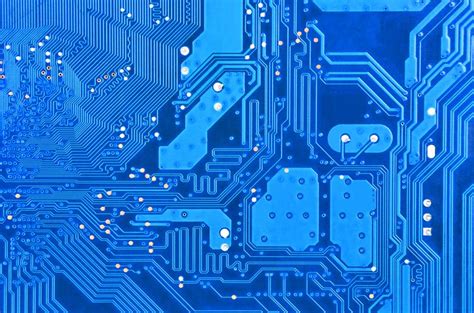
A Printed Circuit Board (PCB) is a fundamental component in modern electronic devices, serving as the backbone that supports and connects various electronic components. At its core, a PCB is a flat, rigid board made from non-conductive material, typically fiberglass, with conductive pathways etched or printed onto its surface.
These pathways, often made of copper, form intricate circuits that allow electrical signals to flow between components such as resistors, capacitors, and integrated circuits. Understanding the basics of PCBs is crucial for anyone involved in electronics, as they are ubiquitous in everything from simple household gadgets to complex industrial machinery.
The design and functionality of PCBs have evolved significantly since their inception.
Initially, electronic circuits were constructed using point-to-point wiring, which was not only labor-intensive but also prone to errors and inconsistencies. The advent of PCBs revolutionized this process by providing a standardized platform for mounting and interconnecting components. This innovation led to increased reliability, reduced manufacturing costs, and the ability to produce more compact and complex electronic devices.
One of the primary advantages of PCBs is their ability to provide a stable and reliable platform for electronic components.
The rigid structure of the board ensures that components remain securely in place, reducing the risk of damage due to physical stress or vibration. Additionally, the use of copper traces to connect components eliminates the need for manual wiring, which can be error-prone and time-consuming. This not only enhances the overall reliability of the circuit but also simplifies the manufacturing process, allowing for mass production of electronic devices.
Another significant benefit of PCBs is their contribution to miniaturization.
As electronic devices become increasingly compact, the need for smaller and more efficient circuit designs has grown. PCBs enable the integration of multiple layers of circuitry within a single board, allowing for more complex and densely packed designs. This multi-layer capability is particularly advantageous in applications where space is at a premium, such as in smartphones, laptops, and medical devices. By stacking layers of circuitry, designers can create highly sophisticated electronic systems without compromising on size or performance.
Moreover, PCBs offer excellent thermal management properties.
Electronic components generate heat during operation, and effective heat dissipation is crucial to maintaining optimal performance and preventing damage. PCBs can be designed with thermal vias and heat sinks to facilitate the efficient transfer of heat away from critical components. This ensures that the device operates within safe temperature limits, thereby extending its lifespan and enhancing its reliability.
In addition to these technical advantages, PCBs also contribute to environmental sustainability.
The standardized manufacturing process of PCBs reduces material waste and energy consumption compared to traditional wiring methods. Furthermore, many modern PCBs are designed with recyclability in mind, allowing for the recovery and reuse of valuable materials such as copper and gold. This not only minimizes the environmental impact of electronic waste but also supports the principles of a circular economy.
In conclusion, Printed Circuit Boards are indispensable in the world of electronics, offering numerous advantages that have transformed the design and manufacturing of electronic devices. Their ability to provide a reliable platform for components, facilitate miniaturization, manage thermal properties, and support environmental sustainability underscores their importance. As technology continues to advance, the role of PCBs will undoubtedly remain central to the development of innovative and efficient electronic systems.
The Evolution Of PCB Technology: A Historical Perspective
Printed Circuit Boards (PCBs) have become an integral component in the realm of modern electronics, serving as the backbone for virtually all electronic devices. To understand the significance of PCBs, it is essential to delve into their historical evolution and the advantages they offer. The journey of PCB technology began in the early 20th century, marking a pivotal shift in the way electronic circuits were designed and manufactured.
Initially, electronic circuits were constructed using point-to-point wiring, a labor-intensive and error-prone method.
This approach involved manually connecting individual components with wires, which often resulted in unreliable connections and bulky designs. The need for a more efficient and reliable method led to the development of the first PCBs in the 1940s. Paul Eisler, an Austrian engineer, is credited with inventing the PCB while working on a radio set during World War II. His innovation laid the groundwork for the mass production of electronic circuits, revolutionizing the electronics industry.
As technology advanced, so did the complexity and capabilities of PCBs.
The introduction of photolithography in the 1950s allowed for more precise and intricate circuit patterns, significantly improving the performance and reliability of electronic devices. This period also saw the transition from single-sided to double-sided and multilayer PCBs, enabling the integration of more components in a compact space. The miniaturization of electronic devices, driven by the demand for portable and high-performance gadgets, further accelerated the evolution of PCB technology.
One of the most significant advantages of PCBs is their ability to provide a stable and reliable platform for electronic components.
The use of a non-conductive substrate, typically made of fiberglass or other insulating materials, ensures that the components are securely mounted and electrically isolated. This reduces the risk of short circuits and enhances the overall durability of the device. Additionally, the copper traces etched onto the substrate create precise and consistent electrical connections, minimizing signal loss and interference.
Another notable advantage of PCBs is their contribution to the miniaturization of electronic devices.
By allowing multiple layers of circuitry to be stacked in a compact form, PCBs enable the design of smaller and more efficient devices. This has been particularly beneficial in the development of consumer electronics, such as smartphones, laptops, and wearable technology, where space is at a premium. Furthermore, the use of surface-mount technology (SMT) has facilitated the placement of smaller components directly onto the PCB, further reducing the size and weight of electronic devices.
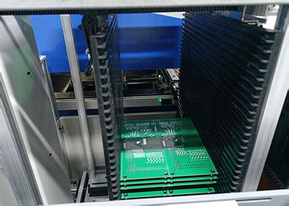
The reliability and ease of manufacturing associated with PCBs have also led to significant cost savings in the production of electronic devices.
Automated assembly processes, such as pick-and-place machines and wave soldering, have streamlined the manufacturing process, reducing labor costs and minimizing human error. This has made it possible to produce high-quality electronic devices at a lower cost, making advanced technology more accessible to consumers.
In conclusion, the evolution of PCB technology has been marked by continuous innovation and improvement, driven by the need for more efficient, reliable, and compact electronic devices. From its humble beginnings with point-to-point wiring to the sophisticated multilayer designs of today, PCBs have transformed the electronics industry. Their numerous advantages, including stability, miniaturization, and cost-effectiveness, have solidified their role as a fundamental component in modern electronics. As technology continues to advance, it is likely that PCB technology will continue to evolve, further enhancing the capabilities and performance of electronic devices.
Key Advantages Of Using PCBs In Modern Electronics
Printed Circuit Boards (PCBs) are the backbone of modern electronic devices, providing a platform for mounting and interconnecting various electronic components. These boards are typically made from non-conductive materials, such as fiberglass or plastic, and are layered with conductive pathways, usually made of copper, to facilitate the flow of electricity. The advent of PCBs has revolutionized the electronics industry, offering numerous advantages that have made them indispensable in the design and manufacturing of electronic devices.
One of the primary advantages of using PCBs is their ability to significantly reduce the size and weight of electronic devices.
Traditional wiring methods, which involved manually connecting components with wires, were not only cumbersome but also prone to errors and inconsistencies. PCBs, on the other hand, allow for the precise and compact arrangement of components, leading to smaller and lighter devices. This miniaturization is particularly crucial in the development of portable electronics, such as smartphones, tablets, and wearable technology, where space is at a premium.
In addition to size reduction, PCBs offer enhanced reliability and durability.
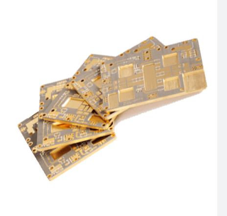
The conductive pathways on a PCB are etched onto the board with high precision, ensuring consistent and reliable connections. This reduces the likelihood of short circuits and other electrical failures that can occur with traditional wiring methods. Furthermore, PCBs are designed to withstand harsh environmental conditions, including extreme temperatures, humidity, and mechanical stress. This robustness makes them suitable for use in a wide range of applications, from consumer electronics to industrial machinery and aerospace systems.
Another significant advantage of PCBs is their ease of mass production.
Once a PCB design is finalized, it can be replicated quickly and efficiently using automated manufacturing processes. This scalability not only reduces production costs but also ensures uniformity and quality across large volumes of products. The ability to produce PCBs in large quantities has been a driving force behind the rapid advancement and widespread adoption of electronic devices in various sectors.
Moreover, PCBs facilitate easier and more efficient troubleshooting and repair.
The organized layout of components and pathways on a PCB allows technicians to quickly identify and isolate faults. Many PCBs also include diagnostic features, such as test points and built-in self-test circuits, which further streamline the troubleshooting process. This ease of maintenance is particularly beneficial in complex systems, where downtime can be costly and disruptive.
The versatility of PCBs is another noteworthy advantage.
They can be designed to accommodate a wide range of components, including resistors, capacitors, transistors, and integrated circuits. This flexibility enables engineers to create custom solutions tailored to specific applications and performance requirements. Additionally, PCBs can be designed with multiple layers, allowing for more complex and sophisticated circuitry within a compact footprint. This multi-layer capability is essential for advanced technologies, such as high-speed computing and telecommunications.
In conclusion, the use of Printed Circuit Boards in modern electronics offers numerous advantages that have made them a cornerstone of the industry. Their ability to reduce size and weight, enhance reliability and durability, facilitate mass production, simplify troubleshooting and repair, and provide design versatility are just a few of the reasons why PCBs are integral to the development and proliferation of electronic devices. As technology continues to evolve, the role of PCBs will undoubtedly remain pivotal, driving innovation and enabling the creation of increasingly sophisticated and efficient electronic systems.
How PCBs Enhance Reliability And Performance In Devices
Printed Circuit Boards (PCBs) are integral components in modern electronic devices, serving as the backbone that supports and connects various electronic components. By providing a structured and reliable platform for electronic circuits, PCBs significantly enhance the reliability and performance of devices. To understand how PCBs achieve this, it is essential to delve into their design, functionality, and the advantages they offer over traditional wiring methods.
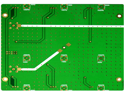
PCBs are composed of a non-conductive substrate, typically made of fiberglass or other insulating materials, onto which conductive pathways are etched or printed.
These pathways, often made of copper, form intricate circuits that interconnect different electronic components such as resistors, capacitors, and integrated circuits. The precision and consistency of these pathways are crucial for the efficient functioning of electronic devices. Unlike traditional wiring, which can be prone to human error and inconsistencies, PCBs are manufactured using automated processes that ensure high levels of accuracy and repeatability.
One of the primary advantages of PCBs is their ability to enhance the reliability of electronic devices.
The fixed and stable connections provided by PCBs reduce the risk of loose or faulty connections, which are common issues in devices that rely on manual wiring. This stability is particularly important in applications where reliability is critical, such as in medical devices, aerospace technology, and automotive systems. By minimizing the potential for connection failures, PCBs contribute to the overall durability and longevity of electronic devices.
In addition to reliability, PCBs also improve the performance of electronic devices.
The compact and organized layout of PCBs allows for the efficient use of space, enabling the design of smaller and more portable devices. This is especially beneficial in the consumer electronics industry, where there is a constant demand for miniaturization. Furthermore, the precise arrangement of components on a PCB reduces the length of electrical paths, thereby minimizing signal delays and enhancing the speed of electronic circuits. This is crucial in high-frequency applications, such as telecommunications and computing, where even minor delays can significantly impact performance.
Another significant advantage of PCBs is their ability to support complex and multi-layered designs.
Modern PCBs can have multiple layers of circuitry stacked on top of each other, separated by insulating layers. This multi-layered approach allows for the integration of more components and more complex circuits within a single board, further enhancing the functionality and performance of electronic devices. The ability to design multi-layer PCBs is particularly valuable in advanced applications, such as in smartphones and advanced computing systems, where high levels of functionality are required within a limited space.
Moreover, PCBs contribute to the ease of manufacturing and assembly of electronic devices.
The standardized design and automated production processes associated with PCBs streamline the manufacturing process, reducing production time and costs. This efficiency is beneficial not only for large-scale production but also for prototyping and small-batch manufacturing, where quick turnaround times are often required.
In conclusion, PCBs play a crucial role in enhancing the reliability and performance of electronic devices. Their precise and stable connections, efficient use of space, support for complex designs, and streamlined manufacturing processes collectively contribute to the superior functionality and durability of modern electronics. As technology continues to advance, the importance of PCBs in the development and production of reliable and high-performing electronic devices will only continue to grow.