What is pcb assembly drawing
Understanding The Basics Of PCB Assembly Drawing
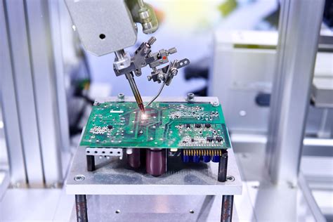
Printed Circuit Board (PCB) assembly drawing is a crucial element in the electronics manufacturing process, serving as a detailed guide for assembling electronic components onto a PCB.
Understanding the basics of PCB assembly drawing is essential for engineers, technicians, and manufacturers to ensure the accurate and efficient production of electronic devices.
This article delves into the fundamental aspects of PCB assembly drawing, elucidating its importance, components, and the role it plays in the overall manufacturing process.
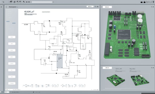
To begin with, a PCB assembly drawing is a comprehensive document that provides visual and textual instructions for placing and soldering components onto a PCB. It typically includes detailed diagrams, component placement information, and assembly notes. The primary purpose of this drawing is to communicate the design intent clearly and unambiguously to the assembly team, thereby minimizing errors and ensuring that the final product meets the desired specifications.
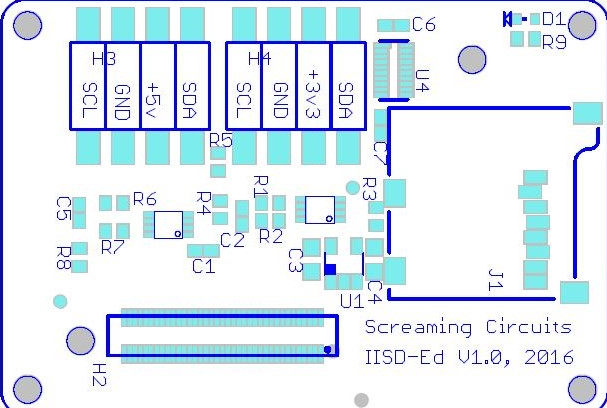
One of the key components of a PCB assembly drawing is the component placement diagram.
This diagram illustrates the exact location of each component on the PCB, often using reference designators to identify individual parts. Reference designators are alphanumeric codes assigned to each component, such as R1 for a resistor or C1 for a capacitor. By providing precise placement information, the component placement diagram helps assemblers position components accurately, which is critical for the functionality and reliability of the final product.
In addition to the component placement diagram, a PCB assembly drawing also includes a bill of materials (BOM).
The BOM is a detailed list of all the components required for the assembly, including part numbers, descriptions, quantities, and supplier information. This list ensures that the assembly team has all the necessary components on hand and can source replacements if needed. Furthermore, the BOM helps in cross-referencing components with their respective reference designators, facilitating a smoother assembly process.
Another vital element of a PCB assembly drawing is the assembly notes section.
Assembly notes provide additional instructions and guidelines that are not easily conveyed through diagrams alone. These notes may include information on soldering techniques, special handling instructions for sensitive components, and any specific requirements for testing and inspection. By including these details, the assembly notes help ensure that the assembly process adheres to the design specifications and quality standards.
Moreover, PCB assembly drawings often incorporate various symbols and annotations to convey additional information.
For instance, polarity markings indicate the correct orientation for polarized components such as diodes and electrolytic capacitors. Similarly, fiducial markers are used as reference points for automated assembly machines, ensuring precise alignment during the placement process. These symbols and annotations play a crucial role in guiding the assembly team and preventing common assembly errors.
Transitioning to the broader context, the importance of PCB assembly drawings cannot be overstated.
They serve as a bridge between the design and manufacturing stages, ensuring that the designer’s intent is accurately translated into a functional product. Without clear and detailed assembly drawings, the risk of assembly errors increases, leading to potential rework, delays, and increased production costs. Therefore, investing time and effort in creating comprehensive PCB assembly drawings is essential for achieving high-quality and reliable electronic products.
In conclusion, understanding the basics of PCB assembly drawing is fundamental for anyone involved in the electronics manufacturing process. By providing detailed diagrams, component placement information, and assembly notes, these drawings ensure that electronic components are accurately and efficiently assembled onto PCBs. As a result, they play a pivotal role in bridging the gap between design and manufacturing, ultimately contributing to the production of high-quality electronic devices.
Key Components Of A PCB Assembly Drawing
A PCB assembly drawing is a crucial document in the electronics manufacturing process, serving as a comprehensive guide for assembling a printed circuit board (PCB). This drawing provides detailed instructions and visual representations to ensure that all components are correctly placed and soldered onto the PCB. Understanding the key components of a PCB assembly drawing is essential for anyone involved in the design, manufacturing, or quality control of electronic devices.
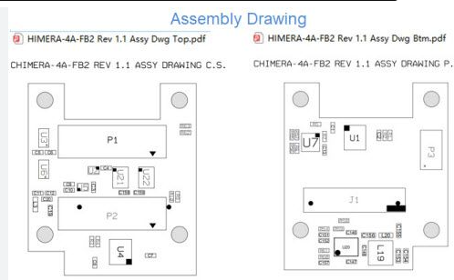
To begin with, a PCB assembly drawing typically includes a detailed layout of the PCB, which shows the exact placement of each component.
This layout is often accompanied by a bill of materials (BOM), listing all the components required for the assembly. The BOM includes information such as part numbers, descriptions, quantities, and reference designators, which correspond to the labels on the PCB layout. This ensures that the correct components are used and helps prevent errors during the assembly process.
In addition to the layout and BOM, a PCB assembly drawing also includes assembly notes.
These notes provide specific instructions and guidelines for assembling the PCB, such as the orientation of polarized components, the type of solder to be used, and any special handling requirements. Assembly notes are crucial for ensuring that the assembly process is carried out correctly and consistently, reducing the risk of defects and improving the overall quality of the final product.
Another key component of a PCB assembly drawing is the solder mask layer.
This layer is a protective coating applied to the PCB to prevent solder from bridging between conductive traces and causing short circuits. The solder mask layer is typically shown in the assembly drawing to indicate areas where solder should not be applied. This helps guide the assembly process and ensures that the solder is applied only where it is needed.
Furthermore, a PCB assembly drawing often includes a silkscreen layer, which provides additional information about the PCB.
The silkscreen layer typically includes labels for components, reference designators, and other markings that help identify the various parts of the PCB. This layer is especially useful during the assembly process, as it helps technicians quickly and accurately identify where each component should be placed.
Moreover, a PCB assembly drawing may also include a mechanical drawing, which provides information about the physical dimensions and mounting requirements of the PCB.
This drawing is essential for ensuring that the assembled PCB fits correctly into its enclosure and interfaces properly with other components in the final product. The mechanical drawing may include details such as hole sizes and locations, board outline dimensions, and mounting hardware specifications.
Additionally, a PCB assembly drawing often includes a test point diagram, which indicates locations on the PCB where electrical tests can be performed.
Test points are used to verify the functionality of the assembled PCB and ensure that it meets the required specifications. The test point diagram helps guide the testing process and ensures that all necessary tests are performed accurately and efficiently.
In conclusion, a PCB assembly drawing is a vital document that provides detailed instructions and visual representations for assembling a printed circuit board. Key components of a PCB assembly drawing include the PCB layout, bill of materials, assembly notes, solder mask layer, silkscreen layer, mechanical drawing, and test point diagram. Understanding these components is essential for ensuring the correct and efficient assembly of PCBs, ultimately leading to high-quality electronic products.
The Importance Of PCB Assembly Drawings In Manufacturing
Printed Circuit Board (PCB) assembly drawings are indispensable in the realm of electronics manufacturing. These detailed documents serve as blueprints for the assembly process, providing critical information that ensures the accurate and efficient production of electronic devices. The importance of PCB assembly drawings cannot be overstated, as they play a pivotal role in bridging the gap between design and manufacturing.
To begin with, PCB assembly drawings offer a comprehensive visual representation of the board layout, including the placement of components, traces, and other essential elements.
This visual guide is crucial for assembly technicians, who rely on it to correctly position and solder components onto the PCB. Without such detailed drawings, the risk of errors increases significantly, leading to potential malfunctions and costly rework. Therefore, these drawings are fundamental in maintaining the integrity and functionality of the final product.
Moreover, PCB assembly drawings provide essential information about the components themselves.
This includes details such as part numbers, reference designators, and orientation marks. These specifics are vital for ensuring that the correct components are used and that they are placed in the right orientation. Misplacement or incorrect orientation of components can lead to short circuits, signal integrity issues, and overall device failure. Thus, the precision and clarity of assembly drawings are critical for the reliability of the electronic device.
In addition to guiding the physical assembly, PCB assembly drawings also facilitate communication between different teams involved in the manufacturing process.
Designers, engineers, and assembly technicians all rely on these drawings to convey their requirements and expectations. This common reference point helps to minimize misunderstandings and ensures that everyone is on the same page. Consequently, the manufacturing process becomes more streamlined and efficient, reducing the likelihood of delays and errors.
Furthermore, PCB assembly drawings are instrumental in quality control and inspection processes.
Inspectors use these drawings to verify that the assembled boards meet the specified design criteria. By comparing the physical board to the assembly drawing, inspectors can quickly identify any discrepancies or defects. This step is crucial for maintaining high standards of quality and ensuring that only fully functional products reach the market. In this way, assembly drawings contribute to the overall reliability and reputation of the manufacturing company.
Another significant aspect of PCB assembly drawings is their role in documentation and traceability.
These drawings serve as a permanent record of the design and assembly process, which can be invaluable for future reference. In the event of a product recall or failure analysis, having detailed assembly drawings allows engineers to trace back and identify potential issues. This documentation is also essential for compliance with industry standards and regulations, which often require thorough records of the manufacturing process.
In conclusion, PCB assembly drawings are a cornerstone of the electronics manufacturing industry. They provide a detailed roadmap for the assembly process, ensuring accuracy, efficiency, and reliability. By offering clear visual guidance, facilitating communication, aiding in quality control, and serving as a vital documentation tool, these drawings play a crucial role in the successful production of electronic devices. As technology continues to advance, the importance of precise and comprehensive PCB assembly drawings will only grow, underscoring their indispensable value in the manufacturing landscape.
Common Mistakes To Avoid In PCB Assembly Drawings
In the realm of electronics manufacturing, PCB assembly drawings serve as a critical blueprint for the successful creation of printed circuit boards. These drawings provide detailed instructions and specifications necessary for assembling the components onto the PCB. However, despite their importance, several common mistakes can occur during the creation of these drawings, potentially leading to costly errors and delays in production. Understanding and avoiding these pitfalls is essential for ensuring a smooth and efficient assembly process.
One prevalent mistake in PCB assembly drawings is the omission of crucial details.
It is imperative to include all necessary information, such as component placements, orientations, and reference designators. Neglecting to provide these details can result in incorrect component placement, leading to malfunctioning boards. Additionally, it is essential to specify the exact locations of components, including their X and Y coordinates, to avoid any ambiguity during assembly. By ensuring that all relevant information is clearly documented, manufacturers can minimize the risk of errors and ensure accurate assembly.
Another common error is the use of outdated or incorrect component libraries.
Component libraries are databases that contain information about various electronic components, including their dimensions, pin configurations, and electrical characteristics. Using outdated or incorrect libraries can lead to mismatched components, causing assembly issues and potential failures. It is crucial to regularly update and verify component libraries to ensure that the information used in the assembly drawings is accurate and up to date. This practice helps to prevent compatibility issues and ensures that the correct components are used during assembly.
Furthermore, inadequate labeling and annotation can also pose significant challenges in PCB assembly drawings.
Clear and concise labeling of components, reference designators, and other relevant information is essential for effective communication between designers and manufacturers. Ambiguous or missing labels can lead to confusion and errors during assembly, resulting in defective boards. It is important to use standardized labeling conventions and ensure that all annotations are legible and unambiguous. By providing clear and consistent labeling, manufacturers can streamline the assembly process and reduce the likelihood of errors.
In addition to labeling, the lack of proper documentation for assembly instructions is another common mistake.
Assembly instructions should be comprehensive and provide step-by-step guidance for the assembly process. This includes details on soldering techniques, component handling, and any specific requirements for certain components. Inadequate or incomplete instructions can lead to improper assembly, resulting in functional issues or even damage to the components. By providing thorough and detailed assembly instructions, manufacturers can ensure that the assembly process is carried out correctly and efficiently.
Moreover, overlooking the importance of design for manufacturability (DFM) considerations can also lead to significant problems in PCB assembly.
DFM involves designing the PCB layout in a way that facilitates efficient and cost-effective manufacturing. Failure to consider DFM principles can result in complex and difficult-to-assemble designs, leading to increased production time and costs. It is crucial to collaborate with manufacturers during the design phase to ensure that the PCB layout is optimized for assembly. By incorporating DFM principles, designers can create designs that are easier to manufacture, reducing the risk of errors and improving overall production efficiency.
In conclusion, avoiding common mistakes in PCB assembly drawings is essential for ensuring a smooth and efficient assembly process. By including all necessary details, using accurate component libraries, providing clear labeling and annotations, documenting comprehensive assembly instructions, and considering DFM principles, manufacturers can minimize errors and improve the quality of the assembled PCBs. These practices not only enhance the reliability and functionality of the final product but also contribute to cost savings and timely production.