What is pcb prototyping
Introduction To PCB Prototyping: Understanding The Basics
Printed Circuit Board (PCB) prototyping is a crucial phase in the development of electronic devices, serving as a preliminary step before mass production. This process involves creating a working model of a PCB to test and validate the design, ensuring that it meets the required specifications and functions correctly. Understanding the basics of PCB prototyping is essential for engineers and designers as it helps in identifying potential issues early in the development cycle, thereby saving time and resources.
To begin with, PCB prototyping starts with the design phase, where engineers use specialized software tools to create a schematic diagram of the circuit.
This schematic serves as a blueprint, detailing the electrical connections and components required for the PCB. Once the schematic is complete, the next step involves converting it into a layout design. This layout specifies the physical arrangement of components on the board and the routing of electrical connections between them. The layout design is critical as it influences the performance, reliability, and manufacturability of the final product.
Following the design phase, the prototype is fabricated.
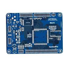
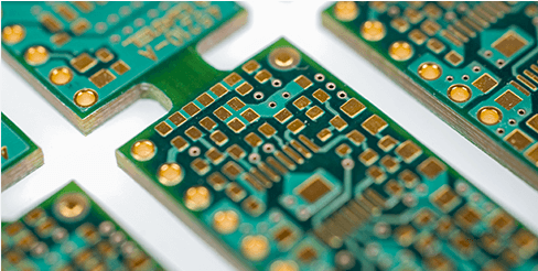
This involves several steps, including the creation of the PCB substrate, the application of conductive traces, and the placement of components. The substrate, typically made of fiberglass or other insulating materials, provides the structural foundation for the PCB. Conductive traces, usually made of copper, are then etched onto the substrate to form the electrical pathways. Components such as resistors, capacitors, and integrated circuits are subsequently mounted onto the board, either through surface-mount technology (SMT) or through-hole technology (THT).
Once the prototype is assembled, it undergoes a series of tests to verify its functionality.
These tests may include electrical testing, where the continuity and integrity of the circuits are checked, as well as functional testing, where the prototype is evaluated under real-world operating conditions. Testing is a critical step in the prototyping process as it helps identify any design flaws or manufacturing defects that could impact the performance of the final product. If issues are detected, the design can be revised and a new prototype can be fabricated for further testing.
In addition to testing, PCB prototyping also involves iterative refinement.
This means that multiple versions of the prototype may be created, each incorporating improvements based on the results of previous tests. This iterative approach allows designers to optimize the PCB design, enhancing its performance, reliability, and cost-effectiveness. Moreover, it provides an opportunity to experiment with different materials, components, and manufacturing techniques, ultimately leading to a more robust and efficient final product.
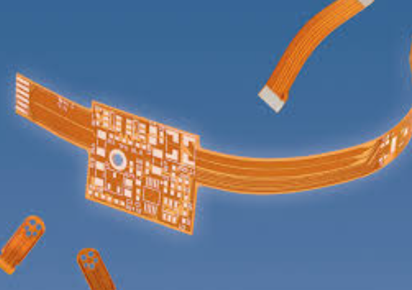
Furthermore, PCB prototyping is not limited to traditional rigid boards.
Flexible PCBs, which can bend and twist without breaking, are increasingly being used in applications where space constraints and mechanical flexibility are important. The prototyping process for flexible PCBs follows similar principles but requires additional considerations for material selection and manufacturing techniques.
In conclusion, PCB prototyping is an indispensable part of the electronic product development process. It enables designers to validate their designs, identify and rectify issues, and optimize the performance and manufacturability of the final product. By understanding the basics of PCB prototyping, engineers can ensure that their designs meet the required specifications and are ready for mass production, ultimately leading to successful and reliable electronic devices.
The Importance Of PCB Prototyping In Electronics Design
Printed Circuit Board (PCB) prototyping is a crucial phase in the electronics design process, serving as a bridge between conceptualization and mass production. This stage involves creating a preliminary version of a PCB to test and validate the design before committing to full-scale manufacturing. The importance of PCB prototyping in electronics design cannot be overstated, as it plays a pivotal role in ensuring the functionality, reliability, and manufacturability of electronic devices.
To begin with, PCB prototyping allows designers to verify the electrical performance of their circuits.
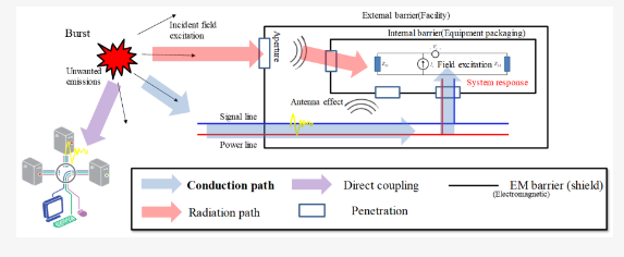
By fabricating a prototype, engineers can conduct a series of tests to ensure that the circuit operates as intended. This step is essential because it helps identify any design flaws or errors that could compromise the performance of the final product. For instance, issues such as signal integrity problems, electromagnetic interference, or incorrect component placement can be detected and rectified during the prototyping phase. Consequently, this reduces the risk of costly revisions and delays in the later stages of production.
Moreover, PCB prototyping facilitates the assessment of the physical layout and mechanical fit of the components.
During the design process, engineers use computer-aided design (CAD) software to create a virtual representation of the PCB. However, translating this digital model into a physical prototype provides a tangible means to evaluate the spatial arrangement of components. This is particularly important for complex designs where space constraints and thermal management are critical considerations. By examining the prototype, designers can make necessary adjustments to optimize the layout, ensuring that components are appropriately spaced and that heat dissipation is effectively managed.
In addition to verifying electrical and mechanical aspects, PCB prototyping also enables the evaluation of the manufacturability of the design.
Manufacturing a PCB involves various processes such as drilling, plating, and soldering, each of which can introduce potential challenges. Prototyping allows engineers to identify and address any manufacturing issues early in the design cycle. For example, they can assess the ease of assembly, the quality of solder joints, and the alignment of multilayer boards. By refining the design based on these insights, engineers can enhance the manufacturability of the final product, leading to higher yields and lower production costs.
Furthermore, PCB prototyping serves as a valuable tool for stakeholder communication and collaboration.
In many cases, the development of electronic products involves input from multiple parties, including designers, engineers, manufacturers, and clients. A physical prototype provides a concrete representation of the design that can be shared and reviewed by all stakeholders. This facilitates effective communication, enabling stakeholders to provide feedback and suggestions for improvement. As a result, the design can be iteratively refined to meet the requirements and expectations of all parties involved.
In conclusion, PCB prototyping is an indispensable step in the electronics design process, offering numerous benefits that contribute to the success of the final product. By enabling the verification of electrical performance, assessment of physical layout, evaluation of manufacturability, and fostering stakeholder collaboration, prototyping helps ensure that the design is robust, reliable, and ready for mass production. As the complexity of electronic devices continues to increase, the importance of PCB prototyping in achieving high-quality and cost-effective designs will only grow, underscoring its critical role in the field of electronics engineering.
Key Steps In The PCB Prototyping Process
PCB prototyping is a crucial phase in the development of electronic devices, serving as a preliminary version of a printed circuit board (PCB) to test and validate the design before mass production. This process involves several key steps, each essential to ensuring the final product meets the desired specifications and functions correctly. Understanding these steps can provide valuable insights into the complexities and precision required in PCB prototyping.
The initial step in PCB prototyping is the design phase, where engineers and designers create a schematic diagram of the circuit.
This schematic serves as a blueprint, detailing the electrical connections and components required for the PCB. Advanced software tools, such as CAD (Computer-Aided Design) programs, are typically employed to facilitate this process, allowing for precise and efficient design work. Once the schematic is complete, it is converted into a layout that specifies the physical arrangement of components on the PCB.
Following the design phase, the next step is to generate the Gerber files, which are the standard file format used in the PCB industry.
These files contain all the necessary information for manufacturing the PCB, including the copper layers, solder mask, and silkscreen layers. The accuracy of these files is paramount, as any errors can lead to defects in the final product. Therefore, thorough verification and validation of the Gerber files are conducted to ensure they align with the design specifications.
Once the Gerber files are prepared, the manufacturing process begins with the fabrication of the PCB.
This involves several sub-steps, starting with the creation of the board’s substrate, typically made from materials like FR4 (a type of fiberglass). The substrate is then coated with a layer of copper, which is etched away to form the circuit pattern. This etching process is highly precise, requiring advanced machinery to achieve the intricate designs specified in the Gerber files.
After the etching process, the PCB undergoes drilling to create holes for component leads and vias
which are essential for establishing electrical connections between different layers of the board. The drilled holes are then plated with copper to ensure conductivity. Following this, a solder mask is applied to protect the copper traces from oxidation and to prevent solder bridges during component assembly. The final step in the fabrication process is the application of the silkscreen layer, which provides labels and markings to assist in component placement and troubleshooting.
With the PCB fabricated, the next phase is assembly, where the electronic components are mounted onto the board.
This can be done using either through-hole technology, where component leads are inserted into drilled holes and soldered, or surface-mount technology (SMT), where components are placed directly onto the surface of the PCB and soldered. SMT is more common in modern electronics due to its efficiency and ability to accommodate smaller components.
The final step in PCB prototyping is testing and validation.
This involves a series of rigorous tests to ensure the PCB functions as intended. Electrical tests, such as continuity and insulation resistance tests, are conducted to verify the integrity of the electrical connections. Functional tests are also performed to ensure the PCB operates correctly within the intended application. Any issues identified during testing are addressed through iterative revisions of the design and manufacturing process.
In conclusion, PCB prototyping is a multifaceted process that encompasses design, file generation, fabrication, assembly, and testing. Each step is critical to the success of the final product, requiring meticulous attention to detail and precision. By understanding these key steps, one can appreciate the complexity and importance of PCB prototyping in the development of reliable and high-quality electronic devices.
Common Challenges And Solutions In PCB Prototyping
PCB prototyping, a crucial phase in the development of electronic devices, involves creating a preliminary version of a printed circuit board to test and validate the design before mass production. Despite its importance, this process is fraught with challenges that can impede progress and affect the final product’s quality. Understanding these common challenges and their solutions is essential for engineers and designers to navigate the complexities of PCB prototyping effectively.
One of the primary challenges in PCB prototyping is the accuracy of the design.
Ensuring that the schematic and layout are error-free is paramount, as even minor mistakes can lead to significant issues in functionality. To address this, thorough design reviews and simulations are indispensable. Utilizing advanced design software that offers real-time error checking and validation can help identify potential problems early in the design phase. Additionally, peer reviews and collaborative design efforts can provide fresh perspectives and catch errors that might have been overlooked.
Another significant challenge is the selection of appropriate materials and components.
The choice of substrate, copper thickness, and components must align with the intended application and operating conditions of the PCB. Inadequate material selection can lead to issues such as signal interference, thermal management problems, and mechanical failures. To mitigate these risks, designers should conduct comprehensive research and consult with material experts to ensure that the chosen materials meet the required specifications. Furthermore, creating a detailed bill of materials (BOM) and sourcing components from reputable suppliers can prevent delays and ensure quality.
Manufacturing tolerances and limitations also pose a considerable challenge in PCB prototyping.
Variations in manufacturing processes can lead to discrepancies between the designed and fabricated PCB, affecting performance and reliability. To overcome this, it is crucial to work closely with the PCB manufacturer during the design phase. Understanding the manufacturer’s capabilities and limitations allows designers to tailor their designs accordingly, ensuring that the final product meets the desired specifications. Additionally, specifying clear and precise manufacturing tolerances in the design documentation can help minimize variations and improve consistency.
Time constraints and cost considerations are perennial challenges in PCB prototyping.
The iterative nature of prototyping, which often involves multiple revisions and testing cycles, can be time-consuming and expensive. To streamline the process, adopting a modular design approach can be beneficial. By breaking down the PCB into smaller, testable modules, designers can isolate and address issues more efficiently. Moreover, leveraging rapid prototyping techniques, such as 3D printing for enclosures and quick-turn PCB services, can significantly reduce lead times and costs.
Testing and validation of the prototype are critical yet challenging aspects of PCB prototyping.
Ensuring that the prototype functions as intended under various conditions requires comprehensive testing, including electrical, thermal, and mechanical assessments. Developing a robust testing plan that outlines specific tests, procedures, and acceptance criteria is essential. Utilizing automated testing equipment and software can enhance accuracy and repeatability, providing reliable data for analysis. Additionally, incorporating feedback from testing into subsequent design iterations is vital for continuous improvement.
In conclusion, PCB prototyping is a complex process that involves navigating numerous challenges, from design accuracy and material selection to manufacturing tolerances, time constraints, and testing. By employing strategic solutions such as thorough design reviews, close collaboration with manufacturers, modular design approaches, and comprehensive testing plans, engineers and designers can effectively address these challenges. Ultimately, overcoming these obstacles ensures the successful development of high-quality, reliable PCBs that meet the intended application requirements.the ever-evolving demands of the electronics industry.