What is PCB side plating?How is PCB side plating designed?
Today,we’ll discuss:PCB side plating,PCB side plating types,and how is PCB side plating designed?
1.What is PCB side plating?
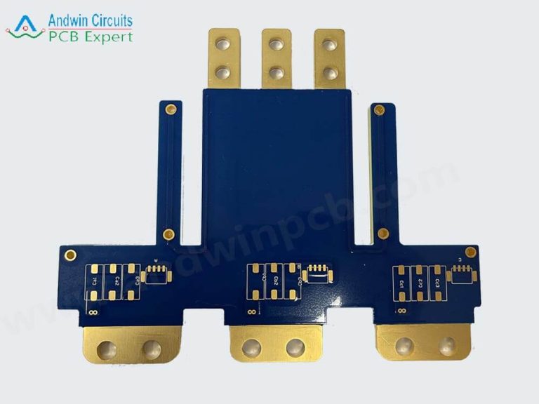
PCB side plating,aslo known as edge plating,is copper plating applied from the top to the bottom surface of the board and along(at least)one peripheral edge.PCB side plating ensures secure connections and reduces the likelihood of device failure,especially for small PCBs and motherboards.Examples of this type of plating are common in WI-FI and Bluetooth modules.
During the manufacturing process,the edges to be metallized should be milled prior to the copper plating process.Appropriate surface treatment is applied to the PCB edge after copper deposition.
2.When is PCB side plating used?
when is edge plating performed?
Need to improve the PCB’s conductivity
Connections are required at the edge of the PCB
The PCB needs protection from lateral impact
A secondary PCB is connected to the main board via the edge
Soldering the edge is required to improve assembly
III. Types of PCB Side Edge Plating
1.Wraparound Edge Plating
Wraparound plating routes the metal edge along the side after drilling. This routing process exposes the PCB sidewall to the electroless base copper so that it can be applied simultaneously with the drill hole.
In the example below, the base layer creates a conductive surface onto which you can electroplate a thicker, more durable copper layer (for better adhesion).
2.Copper Board Edge
To avoid copper damage, a minimum distance between copper features and the PCB edge is typically required. This distance is:
0.25 mm on outer layers with a break
0.40 mm on inner layers with a break
0.45 mm on all layers with a V-cut notch.
The copper-to-board-edge distance should only be used for flat surfaces and large copper areas where even minor damage to the copper will not affect the board’s performance. Tracks should not be located within the minimum distance from the board edge to avoid damage.
If pads are found within the minimum distance from the board edge, they are trimmed back to restore the minimum copper-free space, unless:
The pad is part of an edge connector (typically with a beveled edge)
The pad is marked “to the board edge” on a separate mechanical layer
Trimming more than 25% of the pad surface is considered abnormal in this case.
3.Edge PTH
Edge PTHs are plated holes cut into the edge of a circuit board, also known as butterfly holes, and are used to connect two PCBs via direct soldering or connectors. The edges of the PCB must have sufficient free space to allow the board to be secured in the production panel during manufacturing.
Both the top and bottom layers must have solder pads to securely attach the plating to the board. For smaller sizes, a gold finish is preferred.
Here are some key points to keep in mind:
The edges of the PCB must have sufficient free space to allow the board to be secured in the production panel during manufacturing.
Both the top and bottom layers (and possibly inner layers) must have solder pads to securely attach the plating to the PCB.
As a general rule, holes should be as large as possible to ensure good soldering to the parent PCB; 0.80 mm and larger is recommended.
All finishes are acceptable, but I prefer gold over nickel for smaller sizes.
4.Rounded Edge Plating
Rounded edge plating means that most or part of a PCB or cutout is plated from the top to the bottom. This is primarily used to establish a good ground connection for metal enclosures or shielding purposes. To produce boards with this type of plating, the board outline is milled prior to the through-hole plating process.
Because the plating needs to be fixed within the production panel during processing, 100% edge plating is not feasible. The placement of routing tabs is inherently problematic. For rounded edge plating, electroless nickel gold is the ideal finish.
Here are some key points to note:
A copper strip is required on each side to facilitate the plated connections.
Because the circuit needs to be fixed within the production panel during processing, 100% edge plating is not possible.
Clearly indicate on the mechanical layer where rounded edge plating is required.
Selective electroless nickel gold is the only surface finish suitable for rounded edge plating.
5.How to Design PCB Edge Plating?
(1)PCB Edge Plating Guidelines
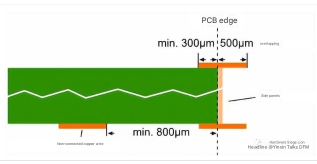
Use overlapping copper to define copper plating areas in the design/layout file. This additional copper deposit can be copper pads, surfaces, or traces.
To ensure the manufacturability of the side panels, metallization areas must be defined in the CAD layout using overlapping copper (copper surfaces, pads, or tracks).
Minimum overlap: 500μm.
On connection layers, a minimum of 500μm is recommended. Connecting copper traces must be defined at 300µm.
On non-connecting layers, copper should have a minimum clearance of 800µm from the outer contour.
2.Metallization Plating Process
This process requires only four steps in the following order: drilling -> milling the metal slot -> removing smear -> electroless copper plating.
External contours requiring metallization must be milled before the through-hole plating process, as the edge metallization occurs during this manufacturing step. After copper deposition, the desired surface finish is finally applied to the edge.
3.Manufacturing Issues
Copper Peeling – On Large Substrates
Plating on surfaces can cause copper peeling due to lack of adhesion. This issue is first addressed by roughening the surface using a combination of chemical and other proprietary methods. Next, direct metallization, which offers higher copper bonding strength, is used to prepare the surface for plating.
Burrs – Edge Plating
Some electroplating processes can produce burrs during final processing. A modified proprietary process is required to polish the burrs to the edge of the feature.
Fab Considerations
Gold pad antennas are too large, interfering with soldering or signal transmission.
Inner edge pads are connected to traces on the board, potentially causing short circuits.
Stamp holes are designed into the edge grinding groove and must be processed during the second drilling process.
Process-dependent manufacturing of individual PCBs as panels makes it impossible to achieve continuous metallization along the outer edges. Metallization should not be applied where small panel bridges exist. Slip-plated metallization can be covered with solder mask.
When purchasing edge-banded boards, it is important to confirm with the PCB supplier whether the PCBs can be manufactured using an electroplating process and the extent to which the manufacturer can perform edge banding. Gerber files or factory drawings should indicate in the mechanical layer where slip plating is required, as well as the required surface finish.
5.Benefits of PCB Edge Plating
- Enhanced Current Conduction
Increasing current-carrying capacity improves the reliability and quality of the board. Furthermore, the correct level of conduction is ideal for components to operate as required and protects vulnerable edge connections.
- Signal Integrity
Edge plating enhances signal integrity by preventing interference from entering the internal electrical pulse transmission.
- Heat Distribution
Because the plated edges are metal, they create additional cooling surface area for dissipating heat to the surrounding air. This metal surface improves the reliability of the board, especially when components are heat-sensitive.
- Better EMC/EMI Performance
Metalized edges allow stray currents to escape, preventing the generation of stray electric and magnetic fields.
- Improved Electromagnetic Compatibility
Edge plating enhances the electromagnetic compatibility of multilayer boards.
- Prevents Static Electricity Damage
When handling circuit boards, static electricity can strike sensitive components, and the metal surface helps absorb it.
6.Applications of PCB Side Edge Plating
Improves EMC performance by shielding multi-layer internal areas (e.g., high-frequency circuit boards)
The edge serves as an additional cooling surface for cooling, enabling active heat dissipation
Enclosure connection
Board-to-board connection (see plated half-holes)
This concludes our knowledge of PCB side edge copper plating.