What is rf circuits pcb
Introduction To RF Circuits PCB: Understanding The Basics
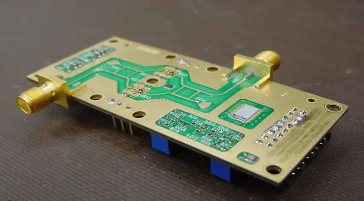
RF circuits PCB, or Radio Frequency circuits printed circuit boards, are specialized types of PCBs designed to operate at radio frequencies, typically ranging from 3 kHz to 300 GHz. These circuits are integral to a wide array of applications, including wireless communication systems, radar systems, and various types of sensors.
Understanding the basics of RF circuits PCB is essential for anyone involved in the design and implementation of high-frequency electronic systems.
To begin with, the fundamental difference between RF circuits PCB and standard PCBs lies in their operational frequency.
While standard PCBs are designed for low-frequency applications, RF circuits PCBs are engineered to handle high-frequency signals with minimal loss and interference. This distinction necessitates a unique approach to their design and fabrication. The materials used in RF circuits PCBs are chosen for their ability to maintain signal integrity at high frequencies. Common materials include PTFE (Polytetrafluoroethylene), Rogers, and other high-frequency laminates, which offer low dielectric loss and stable dielectric constants.
Moreover, the layout of an RF circuits PCB is critical to its performance.
Unlike low-frequency circuits, where the layout might be more forgiving, RF circuits require meticulous attention to detail. The placement of components, the routing of traces, and the grounding techniques all play pivotal roles in minimizing signal loss and electromagnetic interference (EMI). For instance, the use of microstrip or stripline techniques can help control impedance and reduce signal reflections, which are crucial for maintaining signal integrity at high frequencies.
Transitioning to the design considerations, one must also account for the parasitic elements that become significant at RF frequencies.
Parasitic capacitance and inductance can adversely affect the performance of an RF circuit, leading to signal degradation and unwanted resonances. Therefore, designers often employ simulation tools to model these parasitic effects and optimize the PCB layout accordingly. Additionally, the choice of components, such as capacitors, inductors, and resistors, must be compatible with high-frequency operation to ensure reliable performance.
Another important aspect of RF circuits PCB is the thermal management.
High-frequency circuits can generate significant amounts of heat, which, if not properly managed, can lead to thermal drift and component failure. Effective thermal management strategies, such as the use of thermal vias, heat sinks, and proper ventilation, are essential to maintain the longevity and reliability of the RF circuit.
Furthermore, the manufacturing process of RF circuits PCB demands precision and expertise.
The fabrication techniques must ensure tight tolerances and high-quality standards to meet the stringent requirements of RF applications. This includes precise etching of traces, accurate drilling of vias, and careful assembly of components. Any deviation from the specified parameters can result in performance degradation and signal integrity issues.
In conclusion, RF circuits PCB are specialized printed circuit boards designed to operate at high frequencies, necessitating a unique approach to their design, materials, layout, and manufacturing. Understanding these basics is crucial for anyone involved in the development of high-frequency electronic systems. By paying close attention to material selection, layout techniques, parasitic effects, thermal management, and manufacturing precision, one can ensure the optimal performance and reliability of RF circuits PCB in various applications.
Key Design Considerations For RF Circuits PCB
When designing RF circuits on printed circuit boards (PCBs), several key considerations must be taken into account to ensure optimal performance and reliability. RF circuits, which operate at high frequencies, are particularly sensitive to layout, component placement, and signal integrity. Therefore, understanding the nuances of RF PCB design is crucial for engineers and designers.
One of the primary considerations in RF PCB design is the choice of materials.
The substrate material must have a low dielectric constant and low loss tangent to minimize signal attenuation and phase distortion. Common materials include FR-4, Rogers, and Teflon, each offering different properties that can affect the performance of the RF circuit. The selection of the appropriate material is often dictated by the operating frequency and the specific requirements of the application.
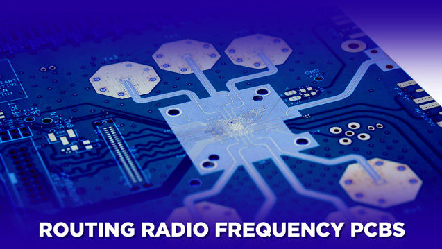
Another critical aspect is the layout of the PCB.
The layout must be meticulously planned to minimize signal loss and interference. This involves careful routing of traces, maintaining consistent impedance, and avoiding sharp bends that can cause signal reflections. Microstrip and stripline techniques are commonly used to control impedance and ensure signal integrity. Additionally, the separation between traces must be sufficient to prevent crosstalk, which can degrade the performance of the RF circuit.
Component placement is equally important in RF PCB design.
Components should be placed in a manner that minimizes the length of signal paths and reduces parasitic inductance and capacitance. This often means placing components as close as possible to each other and to the ground plane. The ground plane itself should be continuous and unbroken to provide a stable reference point and to minimize ground loops, which can introduce noise and signal degradation.
Thermal management is another key consideration.
RF circuits can generate significant amounts of heat, which can affect performance and reliability. Effective thermal management strategies, such as the use of thermal vias, heat sinks, and proper ventilation, are essential to dissipate heat and maintain the integrity of the circuit. The choice of materials and the layout can also influence thermal performance, making it important to consider these factors during the design phase.
Signal integrity is paramount in RF PCB design.
High-frequency signals are susceptible to various forms of interference, including electromagnetic interference (EMI) and radio frequency interference (RFI). Shielding techniques, such as the use of ground planes and metal enclosures, can help mitigate these effects. Additionally, the use of differential signaling and proper termination can further enhance signal integrity by reducing noise and reflections.
Power integrity is also a crucial factor.
RF circuits require stable and clean power supplies to function correctly. Decoupling capacitors should be strategically placed near power pins to filter out noise and provide a stable voltage. The power distribution network (PDN) should be designed to minimize voltage drops and ensure that all components receive the necessary power without introducing noise or interference.
In conclusion, designing RF circuits on PCBs involves a complex interplay of material selection, layout planning, component placement, thermal management, signal integrity, and power integrity. Each of these factors must be carefully considered and optimized to achieve the desired performance and reliability. By paying close attention to these key design considerations, engineers can create RF circuits that meet the stringent demands of high-frequency applications.
Common Challenges In RF Circuits PCB Manufacturing
RF circuits PCB manufacturing presents a unique set of challenges that distinguish it from other types of printed circuit board production. One of the primary difficulties lies in the precise control of impedance. RF circuits operate at high frequencies, where even minor variations in impedance can lead to significant signal loss or distortion. This necessitates meticulous design and manufacturing processes to ensure that the impedance is consistently maintained across the entire PCB. Achieving this level of precision often requires advanced simulation tools and rigorous testing protocols.
Another significant challenge is the management of signal integrity.
High-frequency signals are particularly susceptible to interference and crosstalk, which can degrade the performance of the RF circuit. To mitigate these issues, designers must carefully consider the layout of the PCB, including the placement of components and the routing of traces. Shielding techniques, such as the use of ground planes and guard traces, are often employed to protect sensitive signals from external noise and to minimize the impact of crosstalk between adjacent traces.
Thermal management is also a critical concern in RF circuits PCB manufacturing.
High-frequency components tend to generate more heat, which can affect the performance and reliability of the circuit. Effective thermal management strategies, such as the use of thermal vias and heat sinks, are essential to dissipate heat and maintain the operational stability of the RF circuit. Additionally, the choice of materials plays a crucial role in thermal management. Materials with high thermal conductivity are preferred to facilitate efficient heat dissipation.
Material selection is another area where RF circuits PCB manufacturing diverges from conventional PCB production.
The dielectric properties of the substrate material significantly influence the performance of RF circuits. Materials with low dielectric constant and low loss tangent are typically chosen to minimize signal attenuation and ensure efficient signal transmission. However, these specialized materials can be more expensive and challenging to work with, adding another layer of complexity to the manufacturing process.
Furthermore, the miniaturization trend in electronics poses additional challenges for RF circuits PCB manufacturing.
As devices become smaller, the available space for PCB components and traces is reduced, making it more difficult to maintain the necessary spacing and clearances for high-frequency signals. This requires innovative design solutions and advanced manufacturing techniques to achieve the desired performance within the constraints of limited space.
Quality control is paramount in RF circuits PCB manufacturing.
Given the sensitivity of RF circuits to various factors, even minor defects can have a significant impact on performance. Therefore, rigorous inspection and testing procedures are essential to ensure that the final product meets the required specifications. Advanced testing methods, such as time-domain reflectometry (TDR) and vector network analysis, are often employed to verify the integrity and performance of the RF circuit.
In conclusion, RF circuits PCB manufacturing involves a complex interplay of factors that must be carefully managed to achieve optimal performance.
From impedance control and signal integrity to thermal management and material selection, each aspect presents its own set of challenges. The increasing demand for miniaturized devices further complicates the manufacturing process, necessitating innovative solutions and advanced techniques. Despite these challenges, the meticulous attention to detail and rigorous quality control measures ensure that RF circuits can meet the high-performance standards required in modern electronic applications.
Advanced Techniques For Optimizing RF Circuits PCB Performance
Radio Frequency (RF) circuits are integral to modern communication systems, enabling the transmission and reception of signals over various distances. The performance of these circuits is heavily influenced by the design and fabrication of their printed circuit boards (PCBs). Optimizing RF circuits PCB performance requires a deep understanding of advanced techniques that address the unique challenges posed by high-frequency signals.
One of the primary considerations in optimizing RF circuits PCB performance is the careful selection of materials.
The dielectric constant and loss tangent of the substrate material significantly impact signal integrity. Low-loss materials, such as PTFE (polytetrafluoroethylene) or Rogers laminates, are often preferred for high-frequency applications due to their superior electrical properties. These materials help minimize signal attenuation and phase distortion, ensuring that the RF signals maintain their integrity over the transmission path.
Another critical aspect is the layout of the PCB.
The physical arrangement of components and traces can introduce parasitic inductance and capacitance, which can degrade the performance of RF circuits. To mitigate these effects, designers often employ techniques such as controlled impedance routing and differential pair routing. Controlled impedance routing ensures that the characteristic impedance of the transmission lines matches the source and load impedances, reducing reflections and signal loss. Differential pair routing, on the other hand, helps minimize common-mode noise and crosstalk by ensuring that the two conductors of a differential signal pair are closely coupled and have equal electrical lengths.
Grounding and shielding are also paramount in optimizing RF circuits PCB performance.
A solid ground plane provides a low-impedance return path for RF signals, reducing ground loops and electromagnetic interference (EMI). Additionally, proper grounding techniques, such as via stitching and ground pours, can further enhance signal integrity. Shielding, whether through the use of metal enclosures or PCB-level shielding techniques, helps protect sensitive RF components from external EMI and prevents the emission of unwanted RF energy.
Thermal management is another crucial factor in the performance of RF circuits.
High-frequency components, such as power amplifiers and oscillators, can generate significant heat, which can affect their performance and reliability. Effective thermal management strategies, such as the use of thermal vias, heat sinks, and thermal interface materials, help dissipate heat away from critical components, ensuring stable operation and prolonging the lifespan of the RF circuit.
Moreover, the use of simulation and modeling tools is indispensable in the design and optimization of RF circuits PCBs.
Electromagnetic simulation software allows designers to predict the behavior of RF signals within the PCB, identify potential issues, and make informed design decisions. By simulating the PCB layout and analyzing parameters such as S-parameters, return loss, and insertion loss, designers can optimize the performance of the RF circuit before physical prototyping, saving time and resources.
In addition to these techniques, meticulous attention to detail during the manufacturing process is essential.
Ensuring tight tolerances, precise etching, and accurate component placement can significantly impact the performance of RF circuits. Regular inspection and testing, including techniques such as time-domain reflectometry (TDR) and vector network analysis (VNA), help verify that the fabricated PCB meets the desired specifications and performs as intended.
In conclusion, optimizing RF circuits PCB performance involves a multifaceted approach that encompasses material selection, layout design, grounding and shielding, thermal management, simulation, and meticulous manufacturing practices. By employing these advanced techniques, designers can enhance the performance, reliability, and efficiency of RF circuits, enabling the development of cutting-edge communication systems that meet the demands of modern technology.


