What is rf pcb design
Introduction To RF PCB Design: Key Concepts And Principles
RF PCB design, or Radio Frequency Printed Circuit Board design, is a specialized area within the broader field of PCB design that focuses on the unique challenges and requirements associated with high-frequency signals.
As electronic devices become more sophisticated and wireless communication becomes increasingly prevalent, the demand for effective RF PCB design has grown significantly. Understanding the key concepts and principles of RF PCB design is essential for engineers and designers who aim to create reliable and efficient high-frequency circuits.
One of the fundamental aspects of RF PCB design is the management of signal integrity.
At high frequencies, even minor imperfections in the PCB layout can lead to significant signal degradation. This is due to the fact that RF signals are more susceptible to interference, crosstalk, and signal loss compared to lower-frequency signals. Therefore, careful consideration must be given to the placement and routing of traces, the choice of materials, and the overall layout of the PCB to ensure optimal performance.
Transitioning to the topic of materials, the selection of the right substrate is crucial in RF PCB design.
The dielectric constant (Dk) and loss tangent (Df) of the substrate material directly impact the signal propagation and loss characteristics. Materials with low Dk and Df values are preferred for high-frequency applications as they minimize signal loss and ensure consistent signal speed. Common materials used in RF PCB design include PTFE (Polytetrafluoroethylene), Rogers, and other specialized laminates designed for high-frequency performance.
Another key principle in RF PCB design is impedance control.
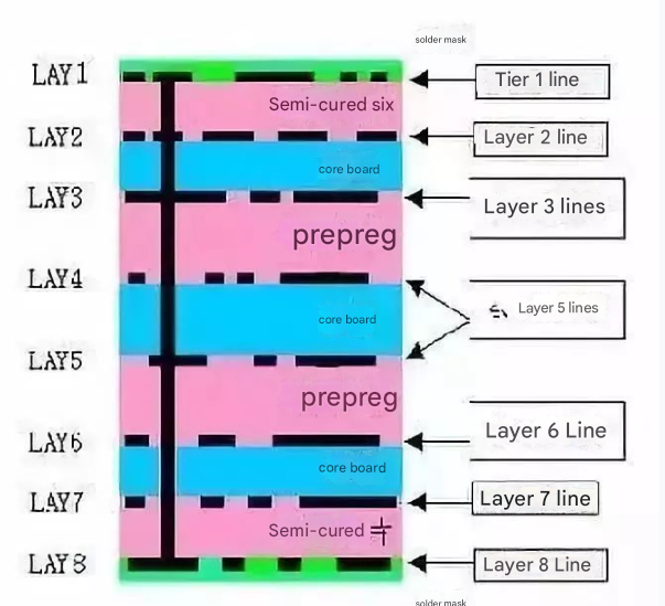
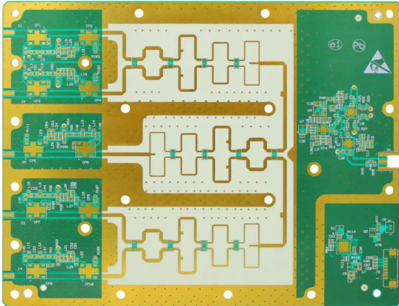
Impedance mismatches can cause signal reflections, leading to signal loss and distortion. To mitigate this, designers must carefully control the impedance of transmission lines, which involves precise calculations and adherence to specific design rules. Microstrip and stripline are two common transmission line structures used in RF PCB design, each with its own set of design considerations. Microstrip lines are routed on the outer layers of the PCB, while stripline structures are sandwiched between layers, providing better shielding and reduced radiation.
Moreover, grounding and shielding play a vital role in RF PCB design.
Effective grounding techniques help to minimize noise and interference, ensuring a clean signal path. This often involves the use of ground planes, which provide a low-impedance path for return currents and help to isolate different sections of the circuit. Shielding, on the other hand, involves enclosing sensitive components or sections of the PCB in conductive materials to protect them from external electromagnetic interference (EMI).
Thermal management is another critical consideration in RF PCB design.
High-frequency circuits can generate significant amounts of heat, which can affect performance and reliability. Proper thermal management techniques, such as the use of thermal vias, heat sinks, and careful component placement, are essential to dissipate heat effectively and maintain the integrity of the RF signals.
In conclusion, RF PCB design is a complex and specialized field that requires a deep understanding of high-frequency signal behavior and meticulous attention to detail. By focusing on signal integrity, material selection, impedance control, grounding, shielding, and thermal management, designers can create PCBs that meet the demanding requirements of modern RF applications. As technology continues to advance, the principles and techniques of RF PCB design will remain critical to the development of reliable and efficient wireless communication systems.
Essential Materials And Components For RF PCB Design
In the realm of RF PCB design, the selection of materials and components is paramount to achieving optimal performance. The intricate nature of radio frequency circuits necessitates a meticulous approach to ensure signal integrity, minimize losses, and maintain the desired frequency response.
To begin with, the choice of substrate material is a critical consideration.
Unlike standard PCBs, RF PCBs often employ substrates with low dielectric constants and low loss tangents, such as PTFE (Polytetrafluoroethylene) or Rogers materials. These substrates are preferred due to their ability to minimize signal attenuation and maintain consistent electrical properties at high frequencies.
Transitioning to the conductive elements, the type of copper used in RF PCB design is equally significant.
High-frequency signals are particularly susceptible to skin effect, where the signal tends to travel on the surface of the conductor. Therefore, using high-purity, smooth copper with minimal surface roughness can reduce signal loss and improve overall performance. Additionally, the thickness of the copper layer must be carefully selected to balance between adequate current-carrying capacity and minimal signal degradation.
Furthermore, the layout and design of transmission lines are crucial in RF PCB design.
Microstrip and stripline configurations are commonly used to guide high-frequency signals. Microstrip lines, which consist of a conductive trace on the top layer of the PCB with a ground plane beneath, are relatively simple to implement but require precise control of trace width and spacing to maintain the desired impedance. Stripline configurations, on the other hand, involve embedding the conductive trace between two ground planes, offering better isolation and reduced electromagnetic interference (EMI). The choice between these configurations depends on the specific application and performance requirements.
In addition to transmission lines, the integration of passive components such as resistors, capacitors, and inductors is essential in RF PCB design.
Surface-mount technology (SMT) components are typically preferred due to their compact size and minimal parasitic effects. However, the placement and orientation of these components must be carefully considered to avoid unwanted coupling and interference. For instance, capacitors used for decoupling should be placed as close as possible to the power supply pins of active devices to ensure effective noise suppression.
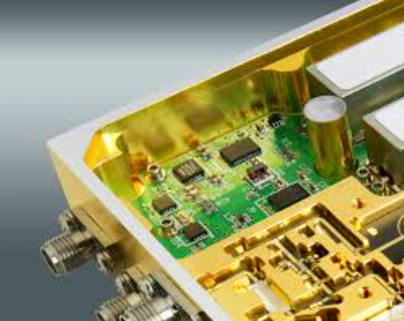
Active components, such as amplifiers, mixers, and oscillators, also play a vital role in RF PCB design.
These components must be selected based on their frequency range, gain, noise figure, and linearity to ensure they meet the specific requirements of the application. Proper thermal management is another critical aspect, as high-frequency components can generate significant heat. Implementing adequate heat sinks, thermal vias, and careful placement of components can help dissipate heat and maintain reliable operation.
Moreover, the use of shielding and grounding techniques is indispensable in RF PCB design to mitigate EMI and crosstalk.
Shielding can be achieved through the use of metal enclosures or ground planes, while proper grounding practices involve creating a low-impedance path for return currents. Ensuring a continuous ground plane and minimizing ground loops can significantly enhance the performance of the RF circuit.
In conclusion, the selection of materials and components in RF PCB design is a multifaceted process that requires careful consideration of various factors. From substrate materials and conductive elements to transmission lines and passive and active components, each element plays a crucial role in achieving the desired performance. By meticulously addressing these aspects and employing effective design practices, engineers can create RF PCBs that meet the stringent demands of high-frequency applications.
Common Challenges And Solutions In RF PCB Design
RF PCB design, or Radio Frequency Printed Circuit Board design, is a specialized area within the broader field of PCB design that focuses on the unique requirements of high-frequency signal transmission. This domain presents a myriad of challenges that are not typically encountered in standard PCB design, necessitating a deep understanding of both the theoretical and practical aspects of RF engineering.
One of the most significant challenges in RF PCB design is signal integrity.
High-frequency signals are particularly susceptible to various forms of interference, including electromagnetic interference (EMI) and crosstalk. These interferences can degrade signal quality, leading to performance issues in the final product. To mitigate these problems, designers often employ techniques such as controlled impedance routing and the use of ground planes. Controlled impedance ensures that the signal traces maintain a consistent impedance, thereby reducing reflections and signal loss. Ground planes, on the other hand, provide a return path for the signals, minimizing EMI and crosstalk.
Another common challenge is the selection of materials.
The dielectric properties of the substrate material can significantly impact the performance of an RF PCB. Materials with low dielectric constant and low loss tangent are generally preferred for high-frequency applications. However, these materials can be more expensive and harder to work with compared to standard FR4 substrates. Therefore, a careful balance must be struck between performance requirements and cost considerations. Additionally, thermal management becomes increasingly critical in RF PCB design. High-frequency components often generate more heat, which can affect both the performance and longevity of the PCB. Effective thermal management strategies, such as the use of thermal vias and heat sinks, are essential to dissipate heat efficiently. Thermal vias are small holes filled with conductive material that help transfer heat from the top layer to the bottom layer of the PCB, while heat sinks provide a larger surface area for heat dissipation.
Component placement is another area where RF PCB design diverges from standard practices.
The placement of components can have a profound impact on signal integrity and overall performance. For instance, placing sensitive components too close to high-frequency signal traces can result in unwanted coupling and interference. Therefore, careful planning and simulation are required to optimize component placement. Simulation tools play a crucial role in addressing many of these challenges. Advanced simulation software can model the electromagnetic behavior of the PCB, allowing designers to identify potential issues before the board is fabricated. These tools can simulate various scenarios, such as different material properties, component placements, and routing strategies, providing valuable insights that can guide the design process.
Moreover, the manufacturing process itself can introduce challenges.
The precision required for RF PCB design often exceeds that of standard PCBs, necessitating tighter tolerances and more stringent quality control measures. Any deviation from the design specifications can result in performance degradation, making it essential to work closely with experienced manufacturers who understand the unique requirements of RF PCBs. In conclusion, RF PCB design is a complex and demanding field that requires a thorough understanding of high-frequency signal behavior, material properties, thermal management, and precise manufacturing techniques. By employing advanced design and simulation tools, carefully selecting materials, and optimizing component placement, designers can overcome these challenges to create high-performance RF PCBs.
Advanced Techniques For Optimizing RF PCB Performance
RF PCB design, or Radio Frequency Printed Circuit Board design, is a specialized field that requires a deep understanding of both electronic principles and the unique challenges posed by high-frequency signals. As the demand for wireless communication and high-speed data transfer continues to grow, optimizing RF PCB performance has become increasingly critical. Advanced techniques are essential to ensure that these circuits function efficiently and reliably.
One of the primary considerations in RF PCB design is the choice of materials.
The substrate material must have low dielectric loss and stable dielectric constant to minimize signal attenuation and phase distortion. Materials such as Rogers or Teflon are often preferred over traditional FR4 due to their superior high-frequency performance. Additionally, the thickness of the substrate and the copper cladding must be carefully selected to balance mechanical strength and electrical performance.
Another crucial aspect is the layout of the PCB.
The placement of components and routing of traces must be meticulously planned to minimize interference and signal degradation. For instance, keeping signal traces as short as possible reduces the potential for signal loss and crosstalk. Moreover, the use of ground planes and proper grounding techniques is vital to provide a return path for signals and to shield sensitive components from electromagnetic interference (EMI).
Transitioning to the topic of impedance matching, it is essential to ensure that the impedance of the transmission lines matches the impedance of the source and load.
Mismatched impedance can lead to signal reflections, which degrade signal integrity and reduce the overall performance of the RF circuit. Techniques such as using microstrip or stripline transmission lines, along with careful calculation and simulation, can help achieve proper impedance matching.
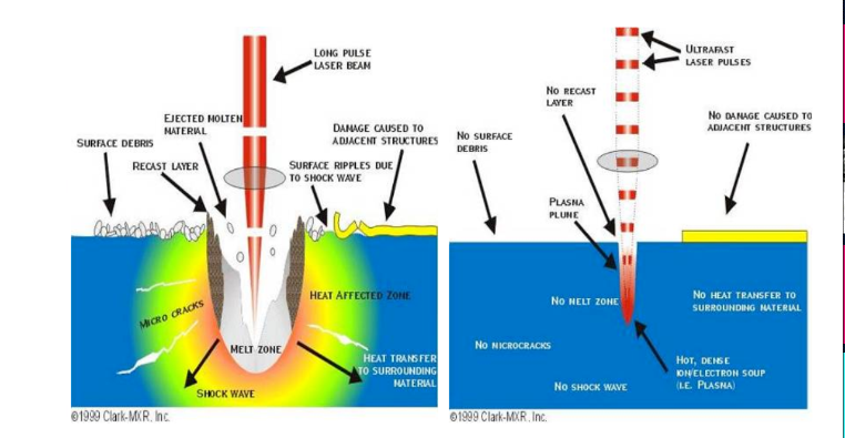
Furthermore, the use of vias in RF PCB design requires careful consideration.
Vias can introduce inductance and capacitance, which can affect signal integrity, especially at high frequencies. To mitigate these effects, designers often use techniques such as via stitching or back-drilling. Via stitching involves placing multiple vias around a signal trace to provide a low-inductance path to the ground plane, while back-drilling removes the unused portion of a via to reduce its inductive effects.
Thermal management is another critical factor in optimizing RF PCB performance.
High-frequency components can generate significant heat, which can affect their performance and reliability. Effective thermal management techniques, such as the use of thermal vias, heat sinks, and proper airflow design, are essential to dissipate heat and maintain the stability of the RF circuit.
In addition to these techniques, simulation and testing play a pivotal role in RF PCB design. Advanced simulation tools, such as electromagnetic field solvers and circuit simulators, allow designers to model and analyze the behavior of their circuits before fabrication. This helps identify potential issues and optimize the design for better performance. Once the PCB is fabricated, rigorous testing, including signal integrity analysis and EMI testing, is necessary to ensure that the design meets the required specifications.
In conclusion, optimizing RF PCB performance involves a combination of material selection, careful layout, impedance matching, via management, thermal management, and thorough simulation and testing. By employing these advanced techniques, designers can create RF circuits that deliver high performance and reliability, meeting the ever-growing demands of modern wireless communication and high-speed data transfer applications.