What is the most direct way to determine the number of PCB layers?
1.Visual inspection
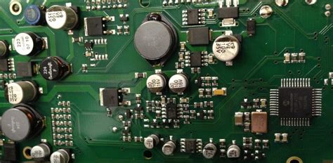
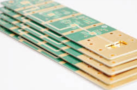
Since the layers in the PCB are tightly combined, it is generally not easy to see the actual number, but if you carefully observe the board fault, you can still distinguish it. If you are careful, we will find that there is one or more layers of white material in the middle of the PCB. In fact, this is the insulation layer between the layers, which is used to ensure that there will be no short circuit between different PCB layers. Because the current multi-layer PCB boards use more single- or double-sided wiring boards, and put an insulation layer between each layer of the board and press it together, the number of layers of the PCB board represents how many independent wiring layers there are, and the insulation layer between the layers has become the most intuitive way for us to judge the number of layers of the PCB.
How to see the number of PCB layers
2.Guide hole and blind hole light method
The guide hole light method uses the “guide hole” on the PCB to identify the number of PCB layers. The principle is mainly because the circuit connection of the multi-layer PCB uses the guide hole technology. If we want to see how many layers the PCB has, we can identify it by observing the guide hole.
On the most basic PCB (single-sided motherboard), the parts are concentrated on one side, and the wires are concentrated on the other side. If you want to use a multi-layer board, you need to punch holes in the board so that the component pins can pass through the board to the other side, so the guide holes will penetrate the PCB board. Therefore, we can see that the pins of the parts are soldered on the other side.
For example, if the board uses a 4-layer board, it is necessary to route on the 1st and 4th layers (signal layers), and the other layers have other uses (ground layer and power layer). The purpose of placing the signal layer on both sides of the power layer and the ground layer is to prevent mutual interference and facilitate correction of the signal line. If some board guide holes appear on the front of the PCB board, but cannot be found on the back, then it must be a 6/8-layer board. If the same guide holes can be found on both sides of the PCB board, it is naturally a 4-layer board.
However, many board manufacturers currently use another routing method, which is to connect only some of the lines, and use buried holes and blind hole technology in the routing. Blind holes connect several layers of internal PCB to the surface PCB without penetrating the entire circuit board.
Buried vias only connect the internal PCB, so they cannot be seen from the surface. Since blind vias do not need to penetrate the entire PCB, if there are six layers or more, the light will not pass through when the board is facing the light source. Therefore, there was a very popular saying before: judge whether the PCB is four-layer or six-layer or more by whether the vias leak light. This method has its reasons, but it is also not applicable. It can be used as a reference method.

3.Accumulation method
To be precise, this is not a method, but an experience. However, this is what we think is the most accurate. We can judge the number of layers of the PCB by the routing and component positions of some public board PCB boards. Because in the current IT hardware industry where the update is so fast, there are not many manufacturers who have the ability to redesign the PCB.
For example, a few years ago, a large number of 9550 graphics cards used a 6-layer PCB design. Careful friends can compare how much difference there is between it and the 9600PRO or 9600XT board type? Only some components are omitted, and the PCB is highly consistent.
In the 1990s, there was a popular saying that the number of PCB layers can be seen by placing the PCB vertically, and many people believed it. This statement was later proved to be nonsense. Even if the manufacturing process at that time was backward, how could the eyes distinguish the distance thinner than a hair? Later, this method continued and modified, and gradually evolved into another measurement method. Now many people believe that the number of PCB layers can be measured with precision measuring instruments such as “vernier calipers”, and we dare not agree with this statement.
Regardless of whether there is such a precision instrument, why can’t we see that the 12-layer PCB is 3 times thicker than the 4-layer one? Different PCBs will use different manufacturing processes, and there is no unified standard for measurement. How to judge the number of layers based on thickness?
In fact, the number of PCB layers has a great impact on the board. For example, why do you need to use at least 6-layer PCBs to install dual CPUs? Because this allows the PCB to have 3 or 4 signal layers, 1 ground layer, and 1 or 2 power layers. Then the signal lines can be far enough apart to reduce interference with each other and have sufficient current supply. However, a 4-layer PCB design is sufficient for general motherboards. Using a 6-layer PCB is too costly and does not provide much performance improvement.