What is the PCB mean?
The full English name of pcb is printed circuit board
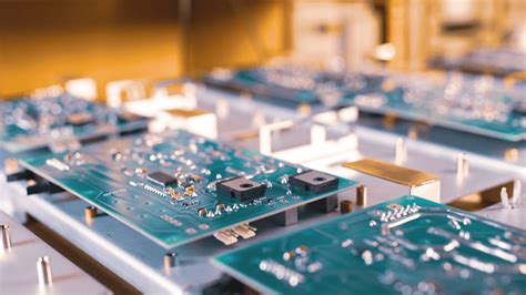
The image of pcb like this:
Pcb board is the abbreviation of printed circuit board ,also named printed circuit board、printed line board ,which is an important electronic component ,a support for electronic components ,and a provider of electronic components. Because it is made by electronic printing,it is also called a “printed circuit board”
History of PCB
The inventor of printed circuit board is paulEisler ,who used a printed circuit board in radio device.In 1943,Americans used this technology extensively in officially recognized this invention for commercial use.In 1948,The united states officially recognized this invention for commercial use.Since the mid-1950s,printed circuit board technology has been widely adopted.
Before the emergence of printed circuit boards the interconnection between electronic components was achieved by direct connection of wires.Now,circuit board only exist as effective experimental tools ,printed circuit boards have occupied an absolute dominant position in the electronics industry.

Pcb design
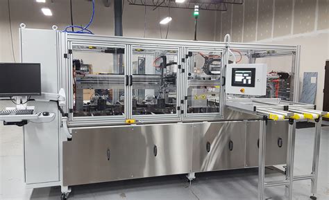
The design of printed circuit boards is based on circuit schematics to achieve the functions required by circuit designers. The design of printed circuit boards mainly refers to layout design, which needs to consider various factors such as the layout of external connections, the optimized layout of internal electronic components, the optimized layout of metal connections and through holes, electromagnetic protection, and heat dissipation. Excellent layout design can save production costs and achieve good circuit performance and heat dissipation performance. Simple layout design can be achieved manually, and complex layout design requires the help of computer-aided design (CAD).

Classification of PCB
According to the number of circuit layers: single-sided boards, double-sided boards, and multi-layer boards. Common multi-layer boards are generally 4-layer boards or 6-layer boards, and complex multi-layer boards can reach more than a dozen layers.
According to soft and hard classification: ordinary circuit boards and flexible circuit boards.
PCB raw materials: copper-clad laminates are substrate materials for making printed circuit boards. It is used to support various components and can achieve electrical connections or electrical insulation between them.
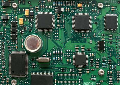
PCB is a printed circuit board (PCB board), which is simply a thin board with integrated circuits and other electronic components.
It appears in almost every electronic device.
According to a recent report by Time magazine, China and India are among the most polluted countries in the world. To protect the environment, the Chinese government has been strictly formulating and implementing pollution control regulations, which have also affected the PCB industry. Many towns are no longer allowed to expand and build new PCB factories, such as Shenzhen. Dongguan has specifically designated four towns as production bases for “polluting industries” and prohibits the construction of new factories outside the designated areas.
If there are electronic parts in a certain device, they are all mounted on PCBs of various sizes. In addition to fixing various small parts, the main function of PCBs is to provide electrical connections between the various parts on it.
As electronic devices become more and more complex, more and more parts are naturally required, and the circuits and parts on PCBs are becoming more and more dense. Bare boards (without parts on them) are also often called “Printed Wiring Boards (PWB)”. The substrate of the board itself is made of insulating and heat-insulating materials that are not easy to bend. The small line material that can be seen on the surface is copper foil. Originally, the copper foil covered the entire board, but part of it was etched away during the manufacturing process, and the remaining part became a mesh of small lines. These lines are called conductor patterns or wiring, and are used to provide circuit connections for components on the PCB.
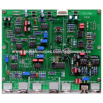
The color of PCB is usually green or brown, which is the color of solder mask. It is an insulating protective layer that can protect copper wires and prevent components from being soldered to incorrect places. A layer of silk screen is also printed on the solder mask. Usually, text and symbols (mostly white) are printed on it to indicate the position of each component on the board.
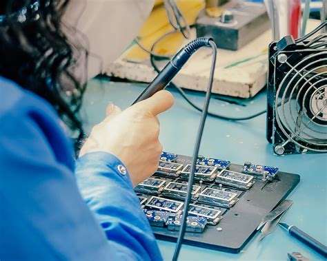
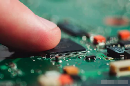
In order to fix the components on the PCB, we solder their pins directly to the wiring. On the most basic PCB (single-sided board), the components are concentrated on one side and the wires are concentrated on the other side. In this way, we need to make holes in the board so that the pins can pass through the board to the other side, so the pins of the components are soldered on the other side. Because of this, the front and back sides of the PCB are called the component side and the solder side.
If there are some parts on the PCB that need to be removed or installed after the production is completed, then a socket will be used when installing the part. Since the socket is directly soldered on the board, the parts can be disassembled and installed at will.
If two PCBs are to be connected to each other, we usually use edge connectors commonly known as “gold fingers”. The gold fingers contain many exposed copper pads, which are actually part of the PCB wiring. Usually when connecting, we insert the gold fingers on one PCB into the appropriate slot on the other PCB (generally called expansion slot). In computers, such as display cards, sound cards or other similar interface cards, they are connected to the motherboard through gold fingers.
The printed circuit board etches the complex circuit copper wires between parts on a board after careful and neat planning, providing the main support for the installation and interconnection of electronic components. It is an indispensable basic part for all electronic products.
A printed circuit board is a flat plate made of non-conductive material. There are usually pre-drilled holes on the plate to install chips and other electronic components. The holes of the components help to connect the pre-defined metal paths printed on the board electronically. After the pins of the electronic components pass through the PCB, they are attached to the PCB with conductive metal welding rods to form a circuit.
Based on their application areas, PCBs can be divided into single-sided boards, double-sided boards, multi-layer boards with more than four layers, and flexible boards. Generally speaking, the more complex the functions of electronic products, the longer the circuit distance, and the more contact pins, the more layers the PCB requires, such as high-end consumer electronics, information and communication products, etc.; and flexible boards are mainly used in products that need to be bent: such as notebook computers, cameras, automotive instruments, etc.
PCB industry chain
According to the upstream and downstream of the industry chain, it can be divided into raw materials-copper clad laminates-printed circuit boards-electronic product applications. The relationship is simply expressed as follows:
Fiberglass cloth: Fiberglass cloth is one of the raw materials of copper clad laminates. It is woven from glass fiber yarn and accounts for about 40% (thick board) and 25% (thin board) of the cost of copper clad laminates. Glass fiber yarn is made of raw materials such as silica sand, which are calcined into liquid in a kiln, and then pulled into extremely fine glass fibers through extremely fine alloy nozzles. Hundreds of glass fibers are then twisted into glass fiber yarn.
The construction investment of the kiln is huge, generally requiring hundreds of millions of funds, and once ignited, it must be produced 24 hours a day, with huge entry and exit costs. Glass fiber cloth manufacturing is similar to weaving companies. The production capacity and quality can be controlled by controlling the rotation speed, and the specifications are relatively simple and stable. There has been almost no significant change in specifications since World War II. Unlike CCL, the price of glass fiber cloth is most affected by supply and demand. The price has fluctuated between US$0.50-1.00/m in recent years. At present, the production capacity of Taiwan and mainland China accounts for about 70% of the world.
Copper foil: Copper foil is the raw material with the largest proportion of the cost of copper clad laminates, accounting for about 30% (thick plates) and 50% (thin plates) of the cost of copper clad laminates. Therefore, the price increase of copper foil is the main driving force for the price increase of copper clad laminates. The price of copper foil is closely reflected in the price change of copper, but the bargaining power is weak. With the recent rise in copper prices, copper foil manufacturers are in a difficult situation. Many companies are forced to close down or be merged. Even if copper clad laminate manufacturers accept the increase in copper foil prices, they are still in a general loss-making state. Due to the emergence of price gaps, there is a high probability that there will be another wave of price increases in the first quarter of 2006, which may drive up CCL prices.
Copper clad laminate: Copper clad laminate is a product of glass fiber cloth and copper foil pressed together with epoxy resin as a fusion agent. It is the direct raw material of PCB and is made into printed circuit boards after etching, electroplating, and multi-layer lamination. The capital demand of the copper clad laminate industry is not high, about 30-40 million yuan, and it can stop production or switch production at any time. In the upstream and downstream industrial chain structure, CCL has the strongest bargaining power. It not only has a strong voice in the procurement of raw materials such as glass fiber cloth and copper foil, but also can pass the pressure of cost increases to downstream PCB manufacturers as long as the downstream demand is acceptable. In the third quarter of this year, copper clad laminates began to increase in price, with a price increase of about 5-8%. The main driving force was to reflect the price increase of copper foil, and the strong downstream demand could absorb the price increase pressure passed on by CCL manufacturers. Nanya, the world’s second largest copper clad laminate manufacturer, also raised its product prices on December 15, showing that at least in the first quarter of 2006, PCB demand was in good shape.
International PCB Industry Development Status
Currently, the global PCB industry output value accounts for more than a quarter of the total output value of the electronic component industry, and is the largest industry in all electronic component sub-industries, with an industry scale of US$40 billion. At the same time, due to its unique position in the electronic basic industry, it has become the most active industry in the contemporary electronic component industry. In 2003 and 2004, the global PCB output value was US$34.4 billion and US$40.1 billion, respectively, with year-on-year growth rates of 5.27% and 16.47%, respectively.
Domestic PCB Industry Development Status
my country’s PCB research and development work began in 1956, and from 1963 to 1978, it gradually expanded to form a PCB industry. Over the past 20 years since the reform and opening up, due to the introduction of foreign advanced technology and equipment, single-sided, double-sided and multi-layer boards have all achieved rapid development, and the domestic PCB industry has gradually developed from small to large. In 2002, China’s PCB output value exceeded Taiwan, becoming the third largest PCB producer. In 2003, the PCB output value and import and export volume exceeded US$6 billion, making it the world’s second largest PCB producer. my country’s PCB industry has maintained a high growth rate of about 20% in recent years, and is expected to surpass Japan around 2010, becoming the country with the largest PCB output value and the most active technological development in the world.
From the perspective of output structure, the main products of China’s PCB industry have shifted from single-sided and double-sided boards to multi-layer boards, and are being upgraded from 4 to 6 layers to 6 to 8 layers or more. With the rapid growth of multi-layer boards, HDI boards, and flexible boards, my country’s PCB industry structure is gradually being optimized and improved.
However, although my country’s PCB industry has made great progress, there is still a large gap compared with advanced countries, and there is still a lot of room for improvement and improvement in the future. First, my country entered the PCB industry relatively late, and there is no specialized PCB R&D institution. There is a big gap with foreign manufacturers in the R&D capabilities of some new technologies. Secondly, from the perspective of product structure, the production of medium and low-layer boards is still the main focus. Although FPC, HDI and other products have grown rapidly, their proportion is still not high due to the small base. Thirdly, most of my country’s PCB production equipment relies on imports, and some core raw materials can only rely on imports. The incompleteness of the industrial chain has also hindered the development of domestic PCB series companies.
PCB industry review
As the most widely used electronic component product, PCB has a strong vitality. Whether judging from the supply and demand relationship or from the historical cycle, the beginning of 2006 is the stage when the industry entered the boom climbing stage. The continued strong downstream demand has driven the shipments of various manufacturers in the PCB industry chain layer by layer, forming a situation of “not off-season” at least in the first quarter of 2006. The industry rating was raised from “avoid” to “good”.