What is thermal relief in pcb
Thermal relief in PCB (Printed Circuit Board) design refers to the use of a pattern of copper pads or traces with small gaps or spokes connecting them to the larger copper planes or traces on the board.
The purpose of thermal relief is to reduce the amount of heat that is transferred from a component to the copper plane or trace,
which can cause the solder to solidify prematurely and lead to poor solder joints.

When a component is soldered onto a PCB, the heat from the soldering iron can cause the copper to expand and contract,
which can create stress on the solder joint. This stress can cause the solder to crack or break, leading to an unreliable connection.
By using thermal relief, the heat is distributed more evenly,
reducing the stress on the solder joint and improving the overall reliability of the connection.
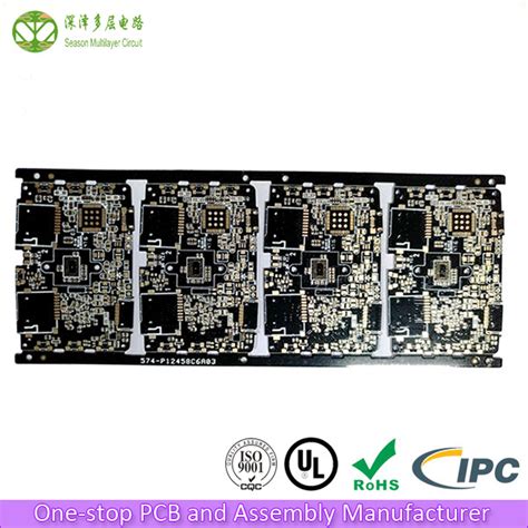
Thermal relief is commonly used in the design of power electronics,
where high currents and temperatures can cause significant stress on the solder joints.
It is also used in other applications where reliable connections are critical, such as aerospace and medical devices.

what does a thermal pad do
A thermal pad is a type of thermal interface material (TIM) that is used to transfer heat between two surfaces.
It is a soft, flexible pad made of a thermally conductive material, such as silicone or graphite, that is placed between a heat-generating component,
such as a CPU or GPU, and a heat sink or cooling solution.
The thermal pad helps to fill any gaps or imperfections between the two surfaces,
ensuring that heat is transferred efficiently and evenly. It also helps to reduce the risk of thermal throttling,
which can occur when a component overheats and slows down to prevent damage.