What is Thermoforming in PCB Assembly?
Introduction to Thermoforming in Electronics Manufacturing
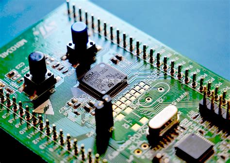
Thermoforming in PCB (Printed Circuit Board) assembly refers to a specialized manufacturing process that involves heating plastic materials to a pliable temperature and forming them into precise three-dimensional shapes that serve as protective enclosures, covers, or specialized components for electronic assemblies. This process plays a critical role in modern electronics manufacturing, particularly for creating customized protective solutions for PCBs and their components.
While thermoforming is widely recognized in packaging industries, its application in PCB assembly represents a more technical and precision-oriented use of the technology. In the context of electronics manufacturing, thermoforming provides numerous advantages including cost-effectiveness, design flexibility, and excellent protective qualities for sensitive electronic components.
The Thermoforming Process in PCB Assembly
Material Selection
The thermoforming process for PCB applications begins with careful material selection. Common materials include:
- PET (Polyethylene Terephthalate): Known for its excellent clarity, strength, and chemical resistance
- PVC (Polyvinyl Chloride): Offers good flexibility and flame retardant properties
- ABS (Acrylonitrile Butadiene Styrene): Provides impact resistance and thermal stability
- Polycarbonate: Delivers superior impact strength and heat resistance
- Conductive or static-dissipative materials: Used for EMI shielding or ESD protection
Material choice depends on factors such as required durability, environmental conditions, thermal properties, and whether the application requires optical clarity for display components.
Heating Phase
In the heating phase, plastic sheets are precisely heated to their forming temperature, typically between 300°F and 400°F (150°C to 200°C), depending on the material. This is accomplished using:
- Conventional ovens: For simpler applications
- Infrared heating systems: For more precise temperature control
- Ceramic heaters: For consistent heat distribution
The heating must be uniform to ensure consistent material properties throughout the forming process.
Forming Techniques
Several thermoforming techniques are employed in PCB assembly:
- Vacuum Forming: The most common method where heated plastic is drawn onto a mold by vacuum pressure
- Pressure Forming: Uses both vacuum and positive air pressure for more detailed features
- Mechanical Forming: Employs matched molds for high-precision parts
- Drape Forming: Suitable for simpler geometries where plastic drapes over a mold
For PCB applications, vacuum and pressure forming are most prevalent due to their ability to create precise features needed for component clearance, connector access, and mounting points.
Trimming and Finishing
After forming, the plastic parts undergo secondary operations:
- Trimming: Excess material is removed using CNC routers, die cutters, or laser cutting systems
- Drilling: Precise holes are added for connectors, mounting hardware, or ventilation
- Surface treatment: May include texturing, painting, or applying conductive coatings
- Quality inspection: Dimensional verification and visual inspection ensure parts meet specifications

Applications of Thermoforming in PCB Assembly
Protective Enclosures
One of the primary uses of thermoforming in PCB assembly is creating protective enclosures that:
- Shield sensitive components from environmental factors (moisture, dust, chemicals)
- Provide mechanical protection against impact and vibration
- Offer EMI/RFI shielding when using conductive materials
- Create IP-rated protective solutions for harsh environments
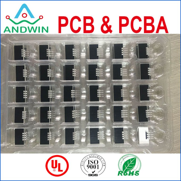
Component Carriers and Trays
Thermoformed plastic is extensively used for:
- PCB carriers during manufacturing and testing
- Shipping trays that protect boards during transportation
- Burn-in test fixtures that hold boards during reliability testing
- Kitting trays that organize components for assembly processes
Specialized Functional Components
Beyond protection, thermoforming creates functional elements such as:
- Light pipes for LED indicators
- Membrane switch overlays
- Touch screen interfaces
- Keyboard components
- Display lenses and covers
Customized Solutions for Unique Requirements
Thermoforming excels at producing:
- Low-volume prototype enclosures
- Custom-shaped EMI shields
- Patient-specific medical device housings
- Conformal covers for irregularly shaped PCBs
Advantages of Thermoforming in PCB Assembly
Cost Effectiveness
Compared to injection molding, thermoforming offers:
- Lower tooling costs (typically 1/5 to 1/10 of injection molds)
- Faster tooling fabrication (days instead of weeks)
- More economical for low to medium production volumes
- Reduced material waste through efficient nesting
Design Flexibility
Thermoforming provides:
- Ability to create large parts from thin-gauge materials
- Freedom to incorporate undercuts and complex geometries
- Easy modification of molds for design iterations
- Capacity to form transparent or opaque materials as needed
Technical Benefits
For PCB applications specifically:
- Excellent dimensional stability for precise component fit
- Good dielectric properties for electrical insulation
- Thermal resistance suitable for most electronic applications
- Chemical resistance against cleaning solvents and environmental exposure
Rapid Prototyping and Time-to-Market
The speed of thermoforming enables:
- Quick design verification with functional prototypes
- Faster transition from design to production
- Ability to test multiple design iterations rapidly
- Shorter lead times for production parts
Challenges and Considerations
Material Limitations
While versatile, thermoforming has some constraints:
- Wall thickness variations in deep draws
- Limited capability for very thick materials
- Potential for webbing in complex geometries
- Material properties may change during forming
Design Considerations
Successful thermoforming for PCB applications requires:
- Proper draft angles for mold release
- Appropriate radiuses to prevent material thinning
- Strategic placement of vents in vacuum forming
- Consideration of material shrinkage during cooling
Quality Control Factors
Key quality aspects include:
- Maintaining consistent wall thickness
- Preventing surface defects like marks or haze
- Ensuring accurate hole placement and sizing
- Verifying dimensional stability over temperature ranges
Comparison with Alternative Technologies
Thermoforming vs. Injection Molding
While injection molding is better suited for:
- Very high volume production
- Parts with extremely complex geometries
- Applications requiring uniform wall thickness
Thermoforming is superior for:
- Larger parts
- Lower volume requirements
- Projects with budget or time constraints
Thermoforming vs. 3D Printing
3D printing offers:
- Greater design freedom without mold constraints
- Ability to create internal structures
- No tooling requirements
But thermoforming provides:
- Faster production times
- Better surface finish
- More cost-effective at moderate volumes
- Wider material selection
Future Trends in PCB Thermoforming
Advanced Materials
Development of new materials with:
- Enhanced thermal conductivity for heat dissipation
- Improved flame retardancy for safety-critical applications
- Better EMI shielding properties
- Self-healing capabilities for scratch resistance
Smart Manufacturing Integration
Incorporation of:
- Industry 4.0 monitoring for process optimization
- Automated quality inspection systems
- AI-driven predictive maintenance for tooling
- Sustainable manufacturing practices
Hybrid Solutions
Combining thermoforming with:
- Insert molding for integrated components
- Additive manufacturing for complex features
- Conductive inks for embedded circuitry
- Multi-material forming for varied properties
Conclusion
Thermoforming in PCB assembly represents a vital manufacturing process that bridges the gap between functional electronics and their physical housing requirements. Its unique combination of cost-effectiveness, design flexibility, and protective capabilities makes it an indispensable technology in electronics manufacturing. As electronic devices continue to evolve toward more compact, customized, and environmentally resistant designs, thermoforming will play an increasingly important role in enabling these advancements while maintaining manufacturing efficiency and reliability.
From simple protective covers to complex functional components, thermoforming offers PCB designers and manufacturers a versatile solution that balances performance, protection, and production economics. As material science advances and manufacturing technologies improve, the applications of thermoforming in PCB assembly will undoubtedly expand, continuing its critical role in electronics manufacturing for years to come.