What processes are required to manufacture PCB printed circuit boards? Easily get PCB design done
1.PCB printed circuit board wiring principles
The principles are as follows:
① The wires used for input and output terminals should be avoided to be adjacent and parallel as much as possible. It is best to add a ground wire between the wires to avoid feedback coupling.
② The minimum width of the printed circuit board wire is mainly determined by the adhesion strength between the wire and the insulating substrate and the current value flowing through them.
When the copper foil thickness is 0.05 mm and the width is 1 to 15 mm, the temperature will not be higher than 3°C when a current of 2 A passes through, so a wire width of 1.5 mm can meet the requirements. For integrated circuits, especially digital circuits, a wire width of 0.02 to 0.3 mm is usually selected. Of course, as long as it is allowed, try to use wide wires, especially power lines and ground wires.
The minimum spacing of the wires is mainly determined by the insulation resistance and breakdown voltage between the wires in the worst case. For integrated circuits, especially digital circuits, as long as the process allows, the spacing can be as small as 5 to 8 um.
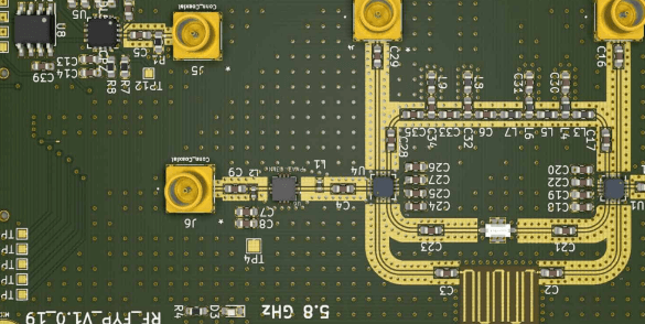
③ The bends of printed conductors are generally in the shape of arcs, while right angles or included angles will affect the electrical performance in high-frequency circuits. In addition, try to avoid using large-area copper foil, otherwise, when heated for a long time, the copper foil is prone to expansion and falling off. When large-area copper foil must be used, it is best to use a grid shape, which is conducive to eliminating the volatile gas generated by the heat of the adhesive between the copper foil and the substrate.

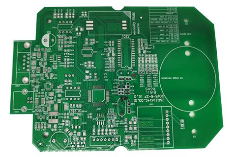
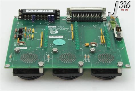
2.PCB manufacturing process
(I) Preliminary preparation
1) Clarify the design goals, select the selected device types, confirm the overall plan, and come up with a written design plan;
2) Prepare the schematic package library and PCB package library of the device. Each component must have a package. If there is no package in the basic library, you must search for it on the Internet. If you still can’t find a ready-made one, you can only draw it yourself. You can use some package generation software to do this work. It should be noted that the package must be placed in the specified directory;
(II) PCB design
This part is the main part of the circuit board design, but if there are problems with the previous plan, it will bring many obstacles to the back, so a good plan is half the success. The next step is to design step by step.
1) Schematic design
The workload of schematic design is not very large, but its importance is unquestionable. A correct schematic is the guarantee of the function of the entire circuit board;
2) Create a schematic netlist
After the schematic is drawn, the netlist must be generated in order to be imported into the PCB drawing software later. If cadence is used, the generated netlist file contains 3 files: pstxnet.dat/ pstxprt.dat/ pstchip.dat;
3) Create mechanical design drawing
Set relevant information such as PCB frame and height limit, generate new mechanical drawing file and save it to the specified directory;
4) Read schematic netlist
Read the schematic netlist into PCB software such as Allegro;
5) Set basic information of PCB board
Before starting layout and routing, be sure to set the board layer, grid spacing, color and design constraints of the PCB board;
6) PCB layout
Except for very simple schematics, it is recommended to perform reasonable manual layout according to the functional distribution of the schematic;
7) PCB routing
Manual routing takes a long time, but is more refined and meets actual requirements; automatic routing is fast but uses more overcontrol. Generally, manual wiring or a combination of the two methods is recommended;
8) Place test points
Place some voltage test points in appropriate locations to facilitate quick testing and confirmation after the circuit board is made;
9) Copper plating on the top and bottom layers
This step is not necessary, but it is performed on almost all mature designs. This not only strengthens the circuit board and prevents warping, but also enhances the shielding performance of the PCB board and improves the anti-interference ability of the PCB board;
10) Constraint rule check
If some constraint rules are designed before layout and wiring, it is necessary to enter the constraint table to check whether all routing designs comply with the rules;
(III) Post-processing
1) Adjust board text
Add and adjust the silk screen, and add some necessary prompt information and company logos on the board;
2) Output photolithography file
Generate a correct photolithography file, and then send it to the plate manufacturer for processing;
3) Document archiving
Common reports include: component list, circuit board interface wiring table, printed circuit schematics and PCB board diagrams.
The above is what I want to share with you about PCB printed circuit boards. I hope you have a certain understanding of the content shared this time. If you want to read articles in different categories, you can select the corresponding channel at the top of the webpage.