What shortcuts can be taken in PCB design? You must read these experiences
In design, layout is an important link. The quality of layout results will directly affect the effect of wiring. Therefore, it can be considered that reasonable layout is the first step to successful PCB design.
Especially pre-layout, it is a process of thinking about the entire circuit board, signal flow, heat dissipation, structure and other architectures. If the pre-layout fails, no matter how much effort is made later, it will be in vain.
1.Consider the overall
The success of a product depends on the internal quality and the overall beauty. Only when both are perfect can the product be considered successful.
On a PCB board, the layout of components must be balanced, dense and orderly, and cannot be top-heavy or heavy.
Will the PCB be deformed?
Is there a process edge reserved?
Is there a MARK point reserved?
Is it necessary to splice the board?
How many layers of boards can ensure impedance control, signal shielding, signal integrity, economy, and feasibility?
2.Eliminate low-level errors
Does the size of the printed board match the size of the processing drawing? Can it meet the PCB manufacturing process requirements? Are there positioning marks?
Are there any conflicts between components in two-dimensional and three-dimensional space?
Are the layout of components dense and orderly, and are they arranged neatly? Are all the components laid out?
Can components that need to be replaced frequently be replaced easily? Is it convenient to insert the plug-in board into the device?
Is there an appropriate distance between thermistors and heating components?
Is it convenient to adjust adjustable components?
Is there a heat sink installed where heat dissipation is required? Is the air flow unobstructed?
Is the signal flow smooth and the interconnection shortest?
Are plugs, sockets, etc. inconsistent with mechanical design?
Have the interference issues of the line been considered?
3.Bypass or decoupling capacitors
When wiring, both analog and digital devices require these types of capacitors, and both need to connect a bypass capacitor close to their power pins. The capacitance value is usually 0.1μF. Keep the pins as short as possible to reduce the inductive reactance of the traces, and keep them as close to the device as possible.
Adding bypass or decoupling capacitors to circuit boards and the arrangement of these capacitors on the board are basic common sense for digital and analog designs, but their functions are different.
In analog wiring design, bypass capacitors are usually used to bypass high-frequency signals on the power supply. If bypass capacitors are not added, these high-frequency signals may enter sensitive analog chips through the power pins. Generally speaking, the frequency of these high-frequency signals exceeds the ability of analog devices to suppress high-frequency signals.
If bypass capacitors are not used in analog circuits, noise may be introduced into the signal path, and in more serious cases, vibration may even be caused. For digital devices such as controllers and processors, decoupling capacitors are also required, but for different reasons.
One function of these capacitors is to act as a “micro” charge reservoir.
This is because in digital circuits, switching of gate states (i.e., switching) usually requires a large current. When switching, switching transient currents are generated on the chip and flow through the circuit board. It is beneficial to have this extra “spare” charge.
If there is not enough charge when performing switching actions, the power supply voltage will change greatly. If the voltage changes too much, the digital signal level will enter an uncertain state and may cause the state machine in the digital device to run incorrectly.
The switching current flowing through the circuit board trace will cause the voltage to change. Since the circuit board trace has parasitic inductance, the voltage change can be calculated using the following formula:
V=Ldl/dt
Where V=voltage change, L=circuit board trace inductance, dI=current change flowing through the trace, dt=current change time.
Therefore, for many reasons, it is a very good practice to apply bypass (or decoupling) capacitors at the power supply or the power pins of active devices.
4.If the input power supply current is relatively large, it is recommended to reduce the trace length and area, and do not run all over the field
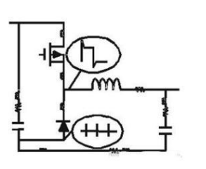
The switching noise on the input is coupled to the plane of the power supply output. The switching noise of the MOS tube of the output power supply affects the input power supply of the previous stage.
If there are a large number of high-current DCDC on the circuit board, there will be different frequencies, high current and high voltage jump interference.
So we need to reduce the area of the input power supply to meet the current flow. Therefore, when laying out the power supply, we should consider avoiding the input power supply running all over the board.
The position of the power line and the ground line is well matched to reduce the possibility of electromagnetic interference (EMl). If the power line and ground line are not properly matched, a system loop will be designed and noise is likely to be generated.
An example of PCB design with improper power line and ground line matching is shown in the figure. On this circuit board, different routes are used to lay the power line and ground line. Due to this improper matching, the electronic components and lines of the circuit board are more likely to be affected by electromagnetic interference (EMI).
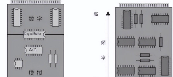
5.Digital-analog separation
In each PCB design, the noisy part and the “quiet” part (non-noise part) of the circuit should be separated.
Generally speaking, digital circuits can tolerate noise interference and are not sensitive to noise (because digital circuits have a larger voltage noise tolerance); on the contrary, the voltage noise tolerance of analog circuits is much smaller. Of the two, analog circuits are most sensitive to switching noise. In the wiring of mixed signal systems, these two circuits should be separated.
6.Heat dissipation considerations
During the layout process, it is necessary to consider the heat dissipation duct and heat dissipation dead corners; heat-sensitive devices should not be placed behind the heat source wind.
Give priority to the layout position of heat dissipation difficult users such as DDR. Avoid repeated adjustments due to failure of thermal simulation.
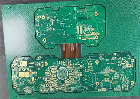
In PCB design, wiring is an important step to complete product design. It can be said that the previous preparations are all done for it. In the entire PCB, the design process of wiring is the most limited, the most skillful, and the most labor-intensive.
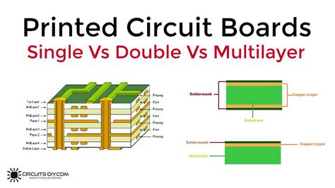
PCB wiring includes single-sided wiring, double-sided wiring, and multi-layer wiring. There are also two ways of wiring: automatic wiring and interactive wiring. Before automatic wiring, you can use interactive wiring to pre-wire the lines with stricter requirements. The edge lines of the input and output ends should avoid adjacent parallel to avoid reflection interference. If necessary, ground wire isolation should be added. The wiring of two adjacent layers should be perpendicular to each other. Parallel wiring is prone to parasitic coupling.
The routing rate of automatic wiring depends on a good layout. The wiring rules can be pre-set, including the number of bends of the routing, the number of vias, the number of steps, etc. Generally, exploratory wiring is first performed to quickly connect the short lines, and then maze wiring is performed. The wiring path of the connection to be routed is optimized globally. It can disconnect the wires that have been routed as needed. And try to re-route to improve the overall effect.
The through hole is not suitable for the current high-density PCB design. It wastes a lot of precious wiring channels. To solve this contradiction, blind hole and buried hole technology have emerged. It not only completes the role of the through hole, but also saves a lot of wiring channels to make the wiring process more convenient, smoother and more perfect. The design process of the PCB board is a complex and simple process. To master it well, it is necessary for the majority of electronic engineering designers to experience it by themselves to get the true meaning.
1.Processing of power supply and ground wire
Even if the wiring in the entire PCB board is completed well, the interference caused by the inconsiderate consideration of the power supply and ground wire will reduce the performance of the product, and sometimes even affect the success rate of the product. Therefore, the wiring of the power and ground wires should be taken seriously, and the noise interference generated by the power and ground wires should be minimized to ensure the quality of the product.
For every engineer engaged in the design of electronic products, they understand the cause of the noise between the ground wire and the power wire. Now only the reduction type suppression of noise is described:
It is well known that decoupling capacitors are added between the power supply and the ground wire.
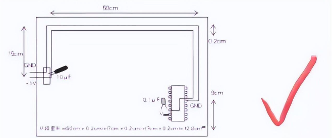
Try to widen the width of the power supply and ground wires. It is best that the ground wire is wider than the power supply wire. The relationship between them is: ground wire > power supply wire > signal wire. Usually the signal wire width is: 0.2~0.3mm, the thinnest width can reach 0.05~0.07mm, and the power supply wire is 1.2~2.5 mm. For the PCB of digital circuits, a wide ground wire can be used to form a loop, that is, to form a ground network for use (the ground of analog circuits cannot be used in this way). Use a large area of copper layer as a ground wire, and connect all unused areas on the printed circuit board to the ground as a ground wire. Or make a multi-layer board, with the power supply and ground wire occupying one layer each.
2. Common ground processing of digital circuits and analog circuits Now many PCBs are no longer single-function circuits (digital or analog circuits), but are composed of a mixture of digital circuits and analog circuits.
Therefore, when wiring, it is necessary to consider the mutual interference between them, especially the noise interference on the ground wire. The frequency of digital circuits is high, and the sensitivity of analog circuits is strong. For signal lines, high-frequency signal lines should be as far away from sensitive analog circuit devices as possible. For ground lines, the entire PCB has only one node to the outside world, so the problem of digital and analog common ground must be handled inside the PCB. In fact, the digital ground and analog ground are separated inside the board. They are not connected to each other, but only at the interface where the PCB is connected to the outside world (such as plugs, etc.).
There is a short circuit between the digital ground and the analog ground. Please note that there is only one connection point. There are also non-common grounds on the PCB, which is determined by the system design.
3.Signal lines are laid on the power (ground) layer
When wiring a multi-layer printed circuit board, since there are not many lines left in the signal line layer, adding more layers will cause waste and increase the workload of production, and the cost will increase accordingly. To solve this contradiction, you can consider wiring on the power (ground) layer.
First, consider using the power layer, and then the ground layer. Because it is best to preserve the integrity of the ground layer.
4.Treatment of connecting legs in large-area conductors
In large-area grounding (electricity), the legs of common components are connected to it. The treatment of connecting legs needs to be comprehensively considered. In terms of electrical performance, it is better for the pads of the component legs to be fully connected to the copper surface, but there are some bad hidden dangers for the welding and assembly of components, such as:
5.Welding requires a high-power heater.
It is easy to cause cold solder joints. Therefore, taking into account both electrical performance and process requirements, a cross-shaped pad is made, which is called heat shield, commonly known as thermal pad (Thermal).
In this way, the possibility of cold solder joints due to excessive heat dissipation in the cross section during welding can be greatly reduced. The treatment of the connecting (ground) layer legs of multilayer boards is the same.
6.The role of network system in wiring
In many CAD systems, wiring is determined by the network system. The grid is too dense, and although the passages have increased, the step is too small, and the amount of data in the drawing field is too large, which will inevitably have higher requirements for the storage space of the equipment, and also have a great impact on the computing speed of computer-related electronic products.
Some paths are invalid, such as those occupied by the pads of the component legs or by the mounting holes and fixed holes. Too sparse grids and too few paths have a great impact on the routing rate. Therefore, a grid system with reasonable density is required to support the routing.
The distance between the two legs of standard components is 0.1 inches (2.54 mm), so the basis of the grid system is generally set to 0.1 inches (2.54 mm) or an integer multiple of less than 0.1 inches, such as: 0.05 inches, 0.025 inches, 0.02 inches, etc.
7.Design Rule Check (DRC)
After the wiring design is completed, it is necessary to carefully check whether the wiring design complies with the rules set by the designer, and also to confirm whether the rules set meet the requirements of the printed circuit board production process. The general inspection includes the following aspects:
Whether the distance between lines, lines and component pads, lines and through holes, component pads and through holes, and through holes is reasonable and meets production requirements.
Are the widths of the power and ground lines appropriate? Are the power and ground lines tightly coupled (low wave impedance)? Is there any place in the PCB where the ground line can be widened?
Have the best measures been taken for key signal lines, such as the shortest length, adding protection lines, and clearly separating the input and output lines?
Do the analog circuits and digital circuits have their own independent ground lines?
Will the graphics added to the PCB later (such as icons and annotations) cause signal short circuits?
Modify some undesirable line shapes.
Are process lines added to the PCB? Does the solder mask meet the requirements of the production process? Is the solder mask size appropriate? Is the character mark pressed on the device pad to avoid affecting the quality of the electrical equipment?
Is the outer frame edge of the power ground layer in the multilayer board reduced? If the copper foil of the power ground layer is exposed outside the board, it is easy to cause a short circuit.
8.Check for sharp angles, impedance discontinuities, etc.
1) For high-frequency currents, when the bends of the wire are at right angles or even sharp angles, the magnetic flux density and electric field strength are relatively high near the bends, which will radiate strong electromagnetic waves, and the inductance here will be relatively large, so the inductive reactance will be larger than that of blunt or rounded angles.
2) For bus wiring of digital circuits, the wiring bends are blunt or rounded, and the area occupied by the wiring is relatively small. Under the same line spacing conditions, the total line spacing width is 0.3 times less than that of right-angle bends.
9.Check the 3W and 3H principles
1) The wiring of clocks, resets, signals above 100M, and some key bus signals and other signal lines must meet the 3W principle, there are no long parallel traces on the same layer and adjacent layers, and the number of vias on the link should be as small as possible.
2) The number of vias for high-speed signals. Some device manuals generally have strict requirements on the number of vias for high-speed signals. The principle of interconnection is that in addition to the necessary pin fanout vias, it is strictly forbidden to drill extra vias in the inner layer. They have laid out 8G PCIE 3.0 routing and drilled 4 vias without any problems.
3) The center distance of clocks and high-speed signals on the same layer must strictly meet 3H (H is the distance from the routing layer to the return plane); signals on adjacent layers are strictly prohibited from overlapping, and it is recommended to meet the principle of 3H. Regarding the above crosstalk problem, there are tools to check.
Routing constraints
Routing constraints: layer distribution Routing constraints: layer distribution
Layered structure of RF single board
Routing constraints: basic requirements
1) The routing requirements are as short as possible, no closed loops, no sharp angles, consistent line width, and no floating lines.
2) Differential signal lines are generally high-speed signals, which must meet the impedance symmetry. Differential lines cannot cross each other, and the line length difference cannot exceed 100mil. The impedance requirements must be met between differential lines and between a single differential line and the ground. The number of differential routing vias cannot exceed 4, and the spacing between differential line pairs must meet the 3W rule.
3) Clock lines, control lines, and electromagnetic sensitive lines are generally prohibited under crystal oscillators, pll filter devices, analog signal processing chips, inductors, and transformers.
4) Analog signals and digital signals, power lines and control signal lines, weak signals and any other signals cannot be routed side by side. They should be layered (preferably with ground isolation) or routed far apart. If the lines of adjacent layers are to be crossed, they cannot be routed in parallel. In order to reduce crosstalk between lines
, the line spacing should be large enough. When the line center spacing is not less than 3 times the line width, 70% of the electric fields can be kept from interfering with each other, which is called the 3W rule. If you want to achieve 98% of the electric fields without interfering with each other, you can use a spacing of 10W. (Note: When routing the clock, you must pay attention to the effective isolation from the data line and the control signal line. The farther the distance, the better. Try not to route them on the same layer.)
5) Strong radiation signal lines (high frequency, high speed, especially clock lines) should not be close to interfaces, handles, etc. to prevent external radiation.
6) Sensitive signals (mainly: weak signals, reset signals, comparator input signals, AD reference power supply, phase-locked loop filter signals, and the filter part of the PLL circuit inside the chip.) The wiring should be as short as possible, not close to strong radiation signals, not placed on the edge of the board, and more than 15mm away from the outer metal frame. When routing long distances, you can wrap the ground (it should be noted that wrapping the ground may cause impedance changes) and inner layer routing. In addition, for the routing of chips with weak ESD, inner layer routing is recommended to reduce the probability of chip damage.
Wiring constraints: power supply
1) Pay attention to power supply decoupling and filtering to prevent interference between different units through power lines. The power lines should be isolated from each other during power wiring. The power lines are isolated from other strong interference lines (such as CLK) by ground lines.
2) The power wiring of small signal amplifiers requires ground copper foil and ground via isolation to prevent other EMI interference from entering, thereby deteriorating the signal quality of this level.
3) Different power layers should avoid overlapping in space. The main purpose is to reduce the interference between different power supplies, especially between some power supplies with large voltage differences. The overlap of power planes must be avoided. If it is difficult to avoid, consider using a ground layer in the middle.
Wiring constraints: power supply overcurrent capacity
1) The number of vias for the power supply conductor printed lines to transfer between layers meets the requirements for the passing current (1A/Ф0.3mm hole)
2) The copper foil size of the POWER part of the PCB meets the maximum current flowing through it, and considers the margin (generally referenced to 1A/mm line width)
Wiring constraints: grounding method
1) The grounding wire should be short and straight to reduce the distributed inductance and reduce the interference caused by the common ground impedance.
Adjust the direction of the filter capacitors in each group to reduce the ground loop. As shown in Figure 15, the grounding of the three filter capacitors is biased towards the direction of the related RF devices, especially the high-frequency filter capacitors.
2) When the grounding devices and power filter capacitors on the RF main signal path need to be grounded, in order to reduce the grounding inductance of the device, it is required to be grounded nearby.
3) The bottom of some components is a grounded metal shell. Some grounding holes should be added in the projection area of the components. Signal lines and vias should not be laid on the surface layer in the projection area;
4) When the grounding line needs to go a certain distance, the line width should be thickened and the line length should be shortened. It is forbidden to approach or exceed 1/4 of the guide wavelength to prevent signal radiation caused by antenna effect;
5) Except for special purposes, there should be no isolated copper skin, and ground vias must be added on the copper skin
6) For some sensitive circuits and circuits with strong radiation sources, they are placed in the shielding cavity respectively. When assembling, the shielding cavity is pressed on the PCB surface. When designing the PCB, a “via shielding wall” should be added, that is, grounding vias should be added to the part of the PCB that is close to the shielding cavity wall. As shown in Figure 12 below, there should be more than two rows of vias, and the two rows of vias are staggered with each other. The spacing between vias in the same row is about 100 mils.
Wiring constraints: general rules
1) The RF signal is routed on the top layer of the PCB, and the plane layer below the RF signal must be a complete ground plane to form a microstrip line structure. As shown in Figure 13. To ensure the structural integrity of the microstrip line, it is necessary to do the following: The microstrip lines in the same layer should be covered with ground copper foil. It is recommended that the edge of the ground copper foil be 3H away from the edge of the microstrip line. H represents the thickness of the dielectric layer. Within the range of 3H, there shall be no other signal vias. It is prohibited for RF signal routing to cross the ground plane gap of the second layer. Ground copper foil should be added between uncoupled microstrip lines, and ground vias should be added on the ground copper foil.
The distance from the microstrip line to the shielding wall should be kept at more than 3H. The microstrip line shall not cross the dividing line of the second layer ground plane.
Microstrip line structure diagram
2) The spacing from the ground copper foil to the signal routing is required to be ≥3H.
3) Add ground holes to the edge of the ground copper foil, with a hole spacing of about 100 mils, and arrange them evenly and neatly;
4) The edge of the ground copper foil should be smooth and flat, and sharp burrs are prohibited;
5) If there are other RF signal lines around the RF signal wiring, add a ground copper foil between the two, and add a ground via every 100 mils on the ground copper foil to isolate them.
6) If there are other irrelevant non-RF signals (such as passing power lines) around the RF signal wiring, add a ground copper foil between the two, and add a ground via every 100 mils.
7) The RF signal via is close to other wiring on the inner layer. For example, the passing power line shown in the left figure is close to the RF signal via. The EMI interference on the power line will penetrate into the RF wiring, so the correct wiring method shown in the right figure of Figure 14 should be adopted. Add a ground and ground via between the power line and the RF signal via to isolate them. Sometimes the inner layer RF signal line is close to other signals with strong interference (such as passing power lines) vias, and the same method is used to add ground vias.
8) When the device mounting hole is a non-metallized hole, the RF signal wiring should be kept away from the device mounting hole. It is necessary to add ground copper foil between the RF signal wiring and the mounting hole, and add ground vias.