What spacings need to be considered in PCB design?
There are many places in PCB design where safety spacing needs to be considered. Here, they are temporarily classified into two categories: one is electrical-related safety spacing, and the other is non-electrical-related safety spacing.
1.Electrical-related safety spacing:
Spacing between wires
According to the processing capabilities of mainstream PCB manufacturers, the spacing between wires must not be less than a minimum of 4mil. The minimum line spacing is also the distance from line to line and from line to pad. From a production perspective, the larger the better if conditions permit, and 10mil is generally more common.
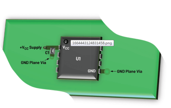
Pad aperture and pad width
According to the processing capabilities of mainstream PCB manufacturers, the minimum pad aperture must not be less than 0.2mm if mechanical drilling is used, and the minimum must not be less than 4mil if laser drilling is used. The aperture tolerance varies slightly depending on the board. It can generally be controlled within 0.05mm. The minimum pad width must not be less than 0.2mm.
Spacing between pads
According to the processing capabilities of mainstream PCB manufacturers, the spacing between pads should not be less than 0.2mm.
Spacing between copper and board edge
The spacing between live copper and PCB board edge should not be less than 0.3mm. As shown in the figure above, set this spacing rule on the Design-Rules-Board outline page.
If it is a large area of copper plating, it is usually necessary to have an indentation distance from the board edge, which is generally set to 20mil. In the PCB design and manufacturing industry, generally speaking, for mechanical considerations of the finished circuit board, or to avoid curling or electrical short circuits caused by copper exposed on the board edge, engineers often indent large area copper blocks by 20mil relative to the board edge, rather than plating copper all the way to the board edge. There are many ways to deal with this copper plating indentation. For example, draw a keepout layer on the board edge, and then set the distance between the copper plating and the keepout. Here is a simple method, which is to set different safety distances for copper objects, such as setting the safety distance of the whole board to 10mil, and setting the copper to 20mil. This can achieve the effect of shrinking the board edge by 20mil. At the same time, it also removes the dead copper that may appear in the device.
2.Non-electrical safety distance:
Character width, height and spacing
No changes can be made to the text film during processing, except that the character line width of D-CODE less than 0.22mm (8.66mil) will be thickened to 0.22mm. That is, the character line width is L0.22mm (8.66mil). The width of the entire character is W1.0mm. The height of the entire character is H1.2mm. The spacing between characters is D0.2mm. When the text is smaller than the above standards, the processing and printing will be blurred.
Via to via spacing (hole edge to hole edge)
The via (VIA) to via spacing (hole edge to hole edge) is preferably greater than 8mil.
Distance from silk screen to pad
Silk screen is not allowed to be on pad. Because if the silk screen covers the pad, the silk screen will not be able to be tinned when tinning, which will affect the installation of components. Generally, the board factory requires a spacing of 8mil. If the PCB board is really limited in area, a spacing of 4mil is barely acceptable. If the silk screen accidentally covers the pad during design, the board factory will automatically eliminate the silk screen part left on the pad during manufacturing to ensure the tinning of the pad.
Of course, the specific situation is analyzed in detail during design. Sometimes the silk screen is deliberately made close to the pad, because when the two pads are close together, the silk screen in the middle can effectively prevent the solder connection from short-circuiting during welding. This situation is another matter.
3D height and horizontal spacing on mechanical structure
When mounting components on PCB, it is necessary to consider whether there will be conflicts with other mechanical structures in the horizontal direction and spatial height. Therefore, when designing, it is necessary to fully consider the adaptability of the spatial structure between components, and between the PCB finished product and the product shell, and reserve a safe distance for each target object. The spacing is considered to ensure that they do not conflict in space.
How to solve the problem of insufficient spacing?
The spacing is measured in air (line of sight), so reasonable layout can be done at the layout level to reduce the required spacing. A significant reduction in spacing can be achieved by using insulating materials and, where possible, by double-sided assembly. The insulating material can be a sheet barrier between high-voltage nodes. Since the high components are surface mounted, circuits that require spacing can be placed on opposite sides of the board. Nodes within the same high-voltage circuit at the same potential usually require attention to spacing from low-voltage circuits. A good approach is to place high-voltage circuits on the top of the board and low-voltage circuits on the bottom for control and monitoring. Low-voltage circuits usually do not have the boundary surface (housing) creepage requirements required by high-voltage circuits.
How to solve the problem of insufficient creepage distance?
As we know, creepage distance is the spacing between electrical nodes on an insulating surface. In our discussion, this means the space between conductors on the surface or internal layers of the PCB. But further expansion of components will be constrained by the product packaging volume, so there needs to be some other strategy to allow higher packaging density while meeting the required creepage distance.
Calculating Standards for Wire Spacing at Various Voltage Levels
Proper distance between PCB traces is critical to avoid short circuits between electrical conductors. Unfortunately, there is no single solution to this problem. Various industrial and safety standards exist that specify different spacing requirements based on voltage, application, and other factors. Here are some considerations to help you determine the proper distance between PCB conductors.
When a product must be certified by a safety agency, each safety testing agency has a set of standards to meet specific insulation requirements. In this case, it is convenient to find the required spacing. For example, in the United States, for most mains or battery-powered information technology equipment, the minimum allowable PCB spacing should be determined according to the standard UL IEC60950-1 2nd edition Table 2K, 2L, 2M or 2N. These tables specify the so-called safety spacing and “creepage distances” for various insulation levels.
The required level depends on the location of the circuit.
When considering the spacing and creepage requirements for a given design, consider the combination of pollution degree and insulation type. Pollution degree generally refers to the amount of dust, moisture, and other particulate matter in the surrounding air or on the surface between high-voltage nodes. The standard specifies functional, basic, supplementary, double, and reinforced insulation. These insulation definitions are quite complex. The creepage distance standards also vary with these insulation levels. The following figure shows the creepage distance required by standard IEC60950-1. The minimum creepage distance required to meet the requirements at different voltage levels. The data in the table below is for basic insulation level. If it is double or reinforced insulation level, the data needs to be doubled.