What to consider when designing PCBs for SiC FETs
Power conversion products have benefited greatly from the introduction of wide bandgap semiconductor switches such as SiC FETs (a normally closed cascode combination of SiC JFETs and silicon MOSFETs). These devices have ultra-fast switching speeds and low conduction losses, which can increase efficiency and power density in a wide range of applications.
However, compared to slower older technologies, high voltage and current edge rates interact more with board parasitic capacitance and inductance, which can generate unwanted induced currents and voltages, resulting in reduced efficiency, component stress, and reliability. In addition, because SiC FET on-resistance is now typically measured in milliohms, PCB trace resistance can be quite large and must be carefully reduced to keep system conduction losses low.
Setting the current edge rate
SiC FETs can easily achieve current edge rates exceeding 1000A/μs (Figure 1), so the inductance around the switching loop between the SiC FET, its load and the local decoupling capacitor will generate transient voltage (Figure 2). For example, according to E = -Ldi/dt, a 100nH loop inductance can generate a transient voltage of 100V, which will increase the device operating voltage, reduce the breakdown margin and increase EMI.
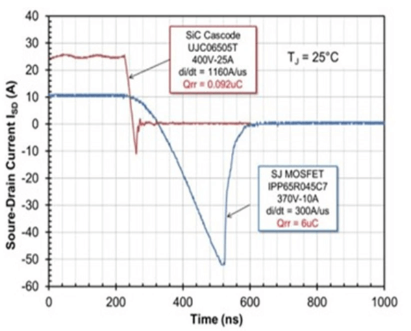
Figure 1: SiC FET switching waveforms showing >1000A/μs edge rates compared to comparable Si SJ MOSFETs
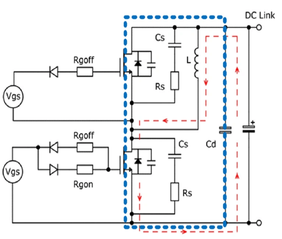
Figure 2: Typical switching loop with high di/dt
This is the true inductance value, and in typical power applications, components cannot be packed close together due to their physical size. For example, a PCB trace of only 50mm (l) produces a total inductance of approximately 100nH for each “go” and “return” connection, calculated from Terman’s equation 1, with a width (W) of 2.5mm and a copper weight (T) of 2oz (0.07mm).
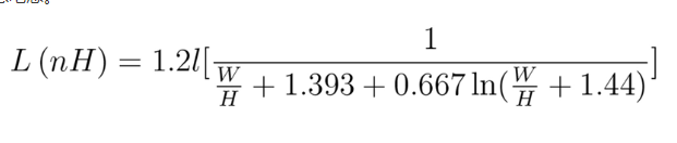
This relationship applies to isolated go and return traces, not to a single trace above the return plane. Interestingly, the graph shows that inductance is relatively independent of trace width and thickness, with length being the dominant factor. (Figure 3)
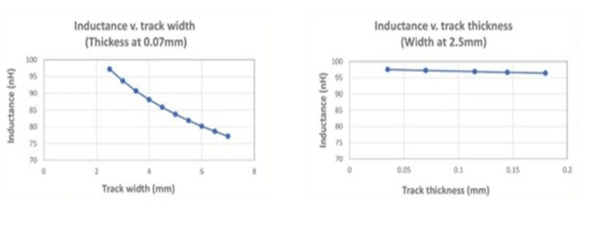
Figure 3: Isolated trace inductance as a function of thickness and width, per Equation 1
The graph shows that the length is shortened and most advantageous by placing the high frequency decoupling capacitor (Cd in Figure 2) closer to the switch than the large DC link capacitor, especially when the capacitor is not a low inductance type. If the departure and return paths are very close, typically using copper planes, then the inductance is greatly reduced (Figure 4).
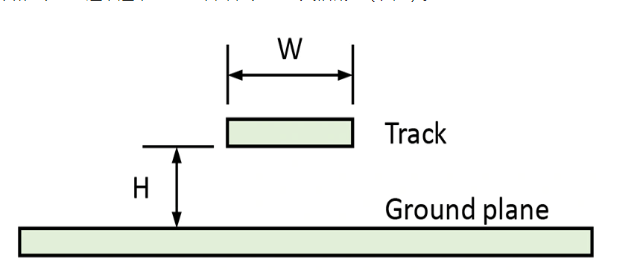
Figure 4: Return plane under the trace significantly reduces total inductance
According to Clayton’s Equation 2, the total loop inductance of a 2.5mm(W) trace with a distance of 1.6mm(H) from the return plane is now only 32nH. The equation is valid for W/H>1 and again, the trace thickness is not a major factor, but now the trace width and the distance between the trace and the plane can have a significant impact (Figure 5). If the return plane is both above and below the trace, the inductance is further reduced with the added benefit of enhanced shielding.
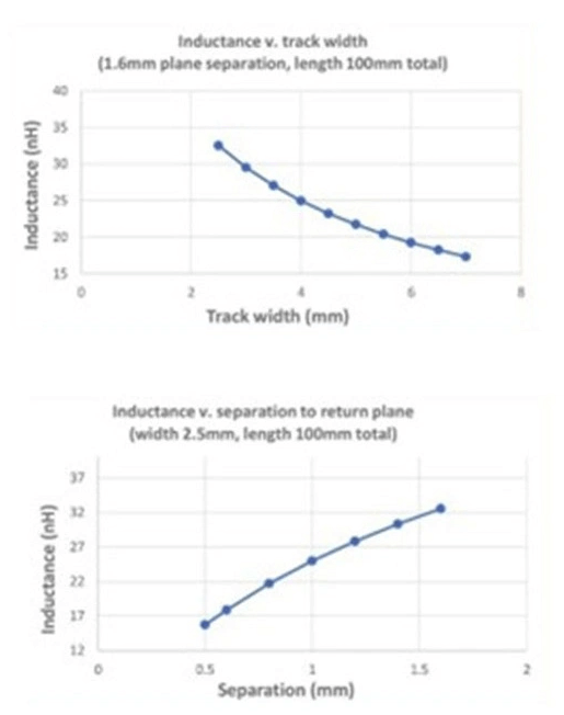
Figure 5: When the return path is a copper plane, the inductance is reduced and varies significantly with the separation distance and trace width
In addition to the traces, vias also increase the inductance and will experience a resistive voltage drop and should be avoided in the power path whenever possible. The inductance of a via depends on the size and whether the hole is filled or not, with an unfilled hole of 0.5mm diameter and 1.6mm length having an inductance of approximately 0.5nH. This value is usually negligible, especially if there are multiple vias in parallel, which may be the case in the power path.
Common connection inductance in gate and source connections is a problem
If the SiC FET gate drive loop and its source current share any length of trace, the inductance of the common connection can generate transient voltages where a load current step acts on the gate drive (Figure 6). In the worst case, the amplitude of the turn-off drive signal is reduced, which can cause “phantom conduction” and “shoot-through” in the bridge converter leg with catastrophic damage. Even with a separate gate drive loop connected to the source of a three-lead TO-247 device, there is still about 10nH of package inductance, which is common and cannot be eliminated, and if the source current edge rate is 1000A/μs, a transient voltage of 10V can be generated. In practical designs, these edge rates are usually slower, and one solution is to use a four-lead device with a separate internal “Kelvin” connection to the source, such as those provided by UnitedSiC (Qorvo). This can reduce the common connection inductance to the die data of about 1nH, allowing higher edge rates and potentially lower dynamic losses.
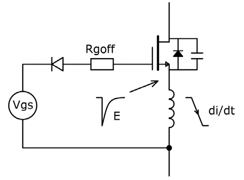
Figure 6: High source di/dt and common connection inductance can generate transient gate voltages
Circuit capacitance can cause unwanted coupling
Note that wider traces are effective in reducing inductance and transient voltages, but they also increase capacitance to adjacent traces, components, and ground. The high dV/dt rates of SiC FETs can cause displacement currents, which can lead to high EMI levels and chaotic operation.
For example, with an edge rate of 100kV/μs, SiC FETs can switch easily, generating 1A through only 10pF. Current flows around the system in routes that are often difficult to identify. At the source connection of the high-side switch, capacitance to the main switch node is a particular problem.
The main switch node can be physically isolated to avoid coupling to any sensitive control or feedback connections. However, there is always a path through the gate driver to the rest of the system, and even if it is isolated magnetically or through an optocoupler, there will be residual capacitance in the signal path and the DC-DC converter that provides the gate drive power. For this reason, care should be taken when specifying isolation components with low coupling capacitance, preferably no more than a few pF.
The capacitance between the switch node and chassis ground is a major source of common-mode EMI that can cause legal limits to be exceeded. Fortunately, the efficiency of devices such as SiC FETs often means that they can be operated with small, ungrounded heat sinks. If a larger, grounded heat sink must be used, an electrostatic shield in the form of copper foil can be used between the switch device and the heat sink, but this will inevitably increase the thermal resistance, so it must be carefully insulated to meet safety standards.
Thermal Considerations
SiC FETs typically have very low losses, so PCB traces and planes can act as heat sinks to keep junction temperatures within reasonable limits. The thermal resistance of such a layout can be difficult to quantify due to interactions with other heat-generating components, so multiphysics simulation software is often used to predict the results. The PCB material, the number of layers and their copper weight, airflow direction and rate, surface emissivity, and cross-heating caused by other components must all be taken into account.
Heat can be transferred through the PCB using thermal vias, an improvement over FR4 with a core thermal conductivity of only about 0.25W/m-K. An unfilled via with a diameter of 0.5mm, a length of 1.6mm and a wall thickness of 0.025mm has a thermal resistance of about 100°C/W (Figure 7).
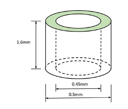
Figure 7: The thermal resistance of a typical via is about 100°C/W. The resistance is about 0.7 milliohms and the inductance is about 0.5nH
As an example, just 12 vias of this size can reduce the thermal resistance from top copper plane to bottom copper plane of a 25mm2, 1.6mm thick PCB area from about 16°C/W to 8°C/W. Insulated metal substrates (IMS) have a thermal resistance of about 45% of FR4, but have the disadvantage of being more expensive and having a practical limit on the number of layers. IMS dielectric thickness is typically around 0.15mm per layer to ensure the lowest possible thermal resistance, which is usually the goal, but does result in relatively high capacitance and, as discussed, can generate high common-mode currents. IMS substrates are generally used in high-density applications to maximize heat removal to the board via liquid or forced air cooling. For non-critical systems with convection cooling, FR4 with thermal vias to the copper plane may be a better fit. As more devices are top-side cooled, the reliance on thermal paths through the PCB is reduced.
Qorvo has demonstrated that simple RC snubber circuits are effective at limiting transient overvoltages generated at the switching edges compared to, for example, slowing the gate drive with a series resistor. Relatively small surface-mount components with very low dissipation can be used to effectively reduce peak voltages. The snubber circuit should be placed as close to the device as possible, using traces of sufficient width to minimize inductance and dissipate the necessary power. Thermal breaks in the form of short “necks” in the traces may help reduce cross-heating generated by the power devices.
PCB trace resistance reduces efficiency
SiC FETs now have an on-resistance of only a few milliohms, even at high voltage ratings, so their conduction losses can be very low. However, the associated trace resistance can be quite large, so it should be minimized to maintain the SiC FET advantage. To assess the impact, PCB resistance depends on copper resistivity, thickness, temperature, and trace length. A convenient way to measure this is to count the number of “squares” along the trace, for example, at 25°C, 35μm/1oz copper has a resistance of 0.5 milliohms per “square” regardless of size, so a 1mm wide, 1mm long trace will have the same resistance as a 10 mil wide, 10 mil long trace. So, as we used in calculating the inductance, a 2.5mm trace with a length of only 100mm would measure 20 milliohms – typically more than the lowest SiC FET on-resistance. Also, copper resistance increases with temperature, in this case to about 26 milliohms at 100°C, so this should be taken into account. The “counting the squares” method is quite accurate for straight traces, but if there are sharp turns, the resistivity will increase at the corners due to current crowding. In any case, right angles should be avoided to prevent local high electric field strengths and increased risk of voltage breakdown.
For AC, the “skin effect” should be considered, whereby as frequency increases, current tends to flow concentrated to the surface rather than flowing within the bulk of the conductor. However, for PCB traces, this effect is typically smaller, with a skin depth of approximately 66/f1/2mm, so even at 1MHz, the switching current flows through a copper depth of 0.07mm or a total thickness of 2oz. Harmonic currents do not penetrate as deeply, but their magnitude is smaller.
When high frequency AC returns through a copper plane, it can be assumed that the resistance on that path is lower. However, since the current is concentrated under the power trace and only the DC component is significantly dispersed, the advantage is not significant (Figure 8).
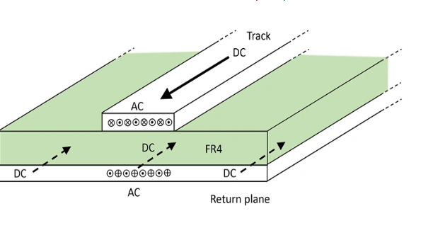
Figure 8: AC return current in the plane is concentrated under the power trace. Any DC component is more dispersed
Conclusion
The actual connection resistance should be understood and reduced in order to fully realize the potential performance of SiC FETs. In some switching topologies, parasitic inductance and capacitance may be part of the resonant tank, so they should also generally be reduced. In this case, it is still important to quantify and control the circuit values.