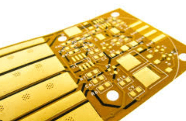
Where are the easy mistakes in PCB design
In basic PCB design, it is easy to ignore the most familiar and simplest places, which leads to errors. This may cause problems or completely break down the perfect PCB circuit diagram when it is converted into a PCB board.
Therefore, in order to assist engineers in reducing design changes and improving work efficiency in PCB board design, Jiepei proposes several easy mistakes in PCB design.
1.Unclear definition of processing level
Single-sided board design is on the TOP layer. If it is not explained whether it is done on the front and back, the board may be installed with devices but not easy to weld.
2.The distance between the large area copper foil and the outer frame is too close
The distance between the large area copper foil and the outer frame should be at least 0.2mm, because when milling the shape, if the copper foil is milled, it is easy to cause the copper foil to warp and the solder resist to fall off.
3.Use filler blocks to draw pads
Using filler blocks to draw pads can pass DRC inspection when designing circuits, but it is not possible for processing, because such pads cannot directly generate solder mask data. When applying solder mask, the filler block area will be covered by solder mask, making it difficult to solder the device.
4.The electrical ground layer is both a flower pad and a connection line
Because the power supply is designed as a flower pad, the ground layer is opposite to the image on the actual printed circuit board, and all the connections are isolation lines. Be careful when drawing several groups of power supplies or several ground isolation lines. Do not leave gaps to short-circuit the two groups of power supplies, nor block the connection area.
5.Random placement of characters
Characters cover the pad SMD solder piece, which brings inconvenience to the printed circuit board continuity test and component welding. If the character design is too small, it will make screen printing difficult, and if it is too large, the characters will overlap and be difficult to distinguish.
6.The pad of the surface mount device is too short
This is for the continuity test. For the surface mount devices that are too dense, the spacing between the two pins is quite small, and the pad is also quite thin. When installing the test pin, the position must be staggered up and down. If the pad is designed to be too short, although it does not affect the installation of the device, it will make the test pin misaligned.
7.Single-sided pad aperture setting
Single-sided pads are generally not drilled. If the drilling needs to be marked, the aperture should be designed to be zero. If the numerical value is designed, the hole coordinates will appear at this position when the drilling data is generated, and problems will occur. Single-sided pads should be specially marked if drilling.
8.Pad overlap
During the drilling process, the drill bit will break due to multiple drillings in one place, resulting in hole damage. Two holes overlap in the multilayer board, and after the negative is drawn, it appears as an isolation disk, resulting in scrap.
9.There are too many filling blocks in the design or the filling blocks are filled with very fine lines
The resulting photo-drawing data is lost, and the photo-drawing data is incomplete. Because the fill block is drawn one by one with lines during photolithography data processing, the amount of photolithography data generated is quite large, which increases the difficulty of data processing.
10.Abuse of graphic layer
Some useless connections are made on some graphic layers. The original four-layer board is designed with more than five layers of circuits, which causes misunderstandings. It violates conventional design. The graphic layer should be kept complete and clear during design.
The above are the ten pitfalls that Jiepei shared with you, which are easy to fall into in PCB design.