Why Are There So Many Via Holes on Power PCBs?
Introduction
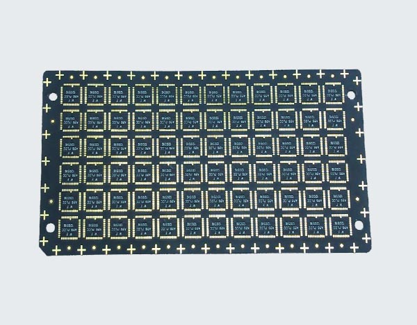
Printed Circuit Boards (PCBs) designed for power applications often feature a distinctive characteristic that may puzzle those unfamiliar with power electronics: an abundance of via holes. These small, plated-through holes that connect different layers of the PCB appear in large numbers, particularly in power supply sections, power planes, and around high-current components. This article explores the multiple technical reasons behind this design practice, examining thermal management, current handling, manufacturing considerations, and electrical performance factors that make via holes essential in power PCB design.
Current Carrying Capacity and Current Distribution
One of the primary reasons for multiple via holes in power PCBs is current handling requirements. In power electronics, currents can be substantial, often reaching tens or even hundreds of amperes. A single via has limited current-carrying capacity, typically in the range of 1-3A depending on its size and plating thickness. To handle higher currents, designers must use multiple vias in parallel.
The current distribution across multiple vias is more uniform than relying on a single large via. This parallel arrangement:
- Reduces current density in any single via
- Minimizes localized heating
- Provides redundancy in case of manufacturing defects in individual vias
- Improves overall reliability under high-current conditions
For example, a power stage needing to carry 30A might use 10-15 vias in parallel, with careful attention to their arrangement to ensure equal current sharing.
Thermal Management Considerations
Power electronics generate significant heat, and vias serve as important thermal pathways. Multiple vias create what designers call “thermal vias” – arrays of holes that conduct heat from power components to other PCB layers or to heatsinking structures.
Key thermal benefits of multiple vias include:
- Heat spreading: Vias transfer heat from hot components to internal planes or opposite board layers
- Reduced thermal resistance: More vias mean lower overall thermal impedance between layers
- Improved heatsinking: Thermal vias connect to external heatsinks or copper areas
- Temperature uniformity: Distributed vias prevent hot spots by evenly spreading heat
In high-power applications, thermal via arrays often appear directly under component pads (like QFN or power MOSFET packages) where they act as heat pipes, conducting heat away from the device junction.
Manufacturing Reliability and Process Considerations
Multiple vias also address various manufacturing and reliability concerns in power PCBs:
Plating uniformity: The electroplating process used to create conductive vias works more consistently with multiple smaller holes rather than few large ones. Large vias may have uneven plating thickness or voids.
Copper balance: PCB fabrication requires relatively symmetrical copper distribution across layers to prevent warping during the high-temperature processes. Multiple small vias help maintain this balance better than few large ones.
Drilling considerations: Small vias (typically 0.2-0.3mm) can be drilled more reliably and at higher speeds than large holes, improving manufacturing yield.
Z-axis expansion: During thermal cycling, the different expansion rates of materials can stress plated through holes. Multiple small vias distribute these stresses more evenly than few large ones.
Electrical Performance Factors
Beyond basic connectivity, multiple vias improve several electrical performance aspects:
Lower inductance: A single via has considerable inductance (typically 0.1-1nH). Multiple vias in parallel reduce overall connection inductance, critical for high-frequency switching currents in power converters.
Improved high-frequency performance: The distributed inductance and capacitance of multiple vias creates a more favorable impedance profile for switching noise and high-frequency currents.
Better return current paths: In multilayer boards, multiple vias provide more options for return currents to find the path of least impedance, reducing ground bounce and EMI.
Reduced voltage drop: The parallel resistance of multiple vias minimizes IR drop in high-current paths.
Via Arrangement Patterns and Design Practices
The arrangement of multiple vias follows several common patterns in power PCB design:
- Grid arrays: Regular rectangular or hexagonal patterns under large components
- Perimeter rings: Circles or rectangles of vias around high-current pads
- Staggered rows: Offset arrangements that maximize via count in limited space
- Density gradients: Higher via concentrations near high-heat or high-current areas tapering to lower densities
Designers must balance via quantity with other constraints:
- Minimum spacing rules for manufacturing
- Maintaining sufficient copper for current paths
- Avoiding solder wicking during assembly
- Thermal expansion considerations
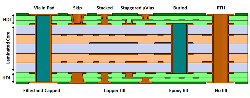
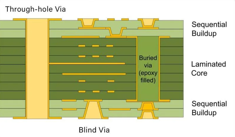
Special Via Types in Power PCBs
Power applications often employ specialized via configurations:
Filled vias: Vias completely filled with conductive material (copper or silver epoxy) for maximum current and thermal capacity
Stacked vias: Multiple aligned vias through different layer pairs for deep thermal paths
Microvias: Very small laser-drilled vias (≤0.1mm) used in high-density interconnect (HDI) power designs
Tented vias: Vias covered with solder mask to prevent solder loss during assembly
Case Studies and Examples
Switch-mode power supply: A 50W DC-DC converter might use 20-30 vias just for the switching MOSFET connections, with additional arrays under the transformer and output rectifiers.
Motor driver PCB: A 20A H-bridge driver could have hundreds of vias distributing current between layers and transferring heat from power devices.
High-current bus bars: Some power PCBs use via “barriers” – dense rows of vias that effectively create vertical current distribution between layers.
Potential Downsides and Mitigations
While multiple vias provide many benefits, they also present some challenges:
Reduced routing space: Vias consume board area that could otherwise be used for traces. Careful layer planning is required.
Solder wicking: During assembly, solder can flow down vias, starving joints. This is mitigated by via tenting, filling, or size control.
Manufacturing cost: While individual vias are inexpensive, very high counts can increase fabrication costs. Optimal via sizing and spacing balances performance and cost.
Thermal stress: The different thermal expansion rates of via barrels and PCB material can cause long-term reliability issues in extreme environments.
Conclusion
The abundance of via holes in power PCBs is not arbitrary but rather a carefully engineered solution to multiple technical challenges. These small interconnects simultaneously address current handling, thermal management, manufacturing reliability, and electrical performance requirements that are particularly demanding in power electronics. By understanding the various roles that multiple vias play – from current sharing to heat spreading to high-frequency performance – designers can implement via strategies that optimize power PCB reliability and performance. As power densities continue to increase in modern electronics, the intelligent use of multiple vias remains an essential tool in the PCB designer’s toolkit.