Why can’t I touch the board with my hand?
It is a common knowledge of electronics engineers that human hands cannot directly touch or touch a circuit board. Why?
First, the harm of static electricity
In different environments, the electrostatic voltage carried by the human body ranges from a few hundred volts to several tens of thousands of volts. Contact with electronic components (conductors) can cause electrostatic discharge, which can damage the device and reduce reliability. In severe cases, electrostatic discharge can cause breakdown of the device and cause the product to be directly scrapped.
In addition, the electrostatic discharge process simultaneously radiates radio waves at a certain frequency, interfering with the peripheral microprocessor, causing the application to run disorderly, which seriously affects the normal operation of the device.
Therefore, in daily production and work, it is necessary to standardize the operation (including the correct wearing of the electrostatic ring); try to avoid direct contact with electronic components, especially in the charged state.
Second, the impact of static electricity on the feedback circuit of the core board
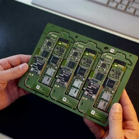
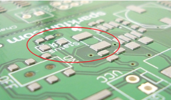
Take the M3352 industrial grade core board (Cortex-A8 core) as an example (the core board passed the electromagnetic compatibility industry level 4 test, including static electricity, surge, pulse group, conducted disturbance, etc.), in the power-on state, the engineer The position of the yellow circle indicated by the finger touch map 4 can induce the system restart phenomenon. What is the reason for this?
The yellow circled area (R80, C116, R79, R78) in Figure 4 is the negative feedback and compensation network (FB part) of the system main power 3.3V DC-DC, as shown in Figure 5.
The human touch (the introduction of interference by the human equivalent resistance) changes the characteristics of the feedback loop (including the offset of the pole), causing the feedback loop to oscillate, resulting in unstable DC-DC output voltage.
The output voltage of the DC-DC is unstable. The light system causes the system to restart (DC-DC automatically reduces the output voltage). In severe cases, the main chip of the board (the DC-DC automatically increases the output voltage) is burned out. .
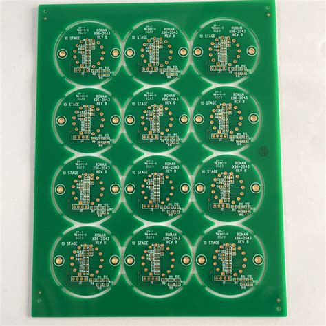
PCB guide hole distinction
The circuit board is made up of a layer of copper foil circuits, and the communication between the different circuit layers depends on the vias. This is because today’s circuit boards are manufactured using drill holes to connect to different circuits. The purpose of the layer, the connection is to conduct electricity, so it is called the via hole. In order to conduct electricity, a conductive material (usually copper) must be electroplated on the surface of the hole, so that the electron can be in different copper. The foil layers move between them because the surface of the original drilled hole is only electrically non-conductive.
Generally, there are three kinds of PCB vias (Via) that we often see, which are described as follows:
Through Hole: Plating Through Hole Abbreviation PTH
This is the most common type of via hole. You just need to pick up the PCB and look at the light. You can see that the light hole is a “through hole.” This is also the simplest kind of hole, because it is only necessary to use the drill bit or laser light to drill the board directly, and the cost is relatively cheap. Although the through hole is cheap, sometimes it will use more PCB space. For example, we have a six-story house. I bought it on the third and fourth floors. I want to design a staircase inside, only between the third and fourth floors. For me, the space on the fourth floor. Invisibly, it was used by the original first floor to connect to the stairs on the sixth floor.
Blind hole: Blind Via Hole (BVH)
The outermost circuit of the PCB is connected to the adjacent inner layer by a plated hole, and since it is not visible, it is called a “blind hole”. In order to increase the space utilization of the PCB circuit layer, a “blind hole” process has emerged. This method of production requires special attention to the depth of the drill hole (Z-axis). It is just right to drill the hole in the individual circuit layers before the circuit layer that needs to be connected, and finally glue it together, but it requires precise positioning. And alignment device. As an example of buying a building above, a six-story house is only connected to the first floor and the second floor, or the stairs connecting from the fifth floor to the sixth floor are called blind holes.
Buried hole: Buried Via Hole (BVH)
The connection of any circuit layer inside the PCB is not conducted to the outer layer. This process can not be achieved by means of bonding after drilling. It is necessary to perform drilling at the time of individual circuit layers. After partially bonding the inner layer, it must be electroplated first, and finally it can be fully bonded, compared with the original “through hole”. The “blind hole” takes more time, so the price is also the most expensive. This process is typically only used on high-density (HDI) boards to increase the usable space of other circuit layers. As an example of buying a building above, a six-story house has only a staircase connecting the third floor and the fourth floor, which is called a buried hole.
e