Why can’t the signal line change holes multiple times in high-speed PCB design?
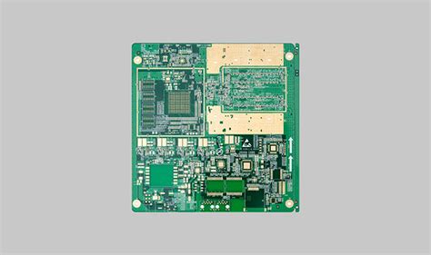
Why can’t the signal line change holes multiple times in high-speed PCB design? Everyone must have come into contact with vias when designing PCBs, so everyone knows that vias have a great impact on the quality of PCB signals. Let me first introduce to you how to select vias when designing PCBs.
8/16±2mil 10/20±2mil 12/24±2mil
Usually, when the board is dense, we will use 8/16±2mil (8/14, 8/16, 8/18) size vias. When the board is relatively empty, you can choose 12/24±2mil (12/22, 12/24, 12/26) size vias. Between 10/20, you can use 10/20±2mil (10/18, 10/20, 10/22) size vias.
In terms of economic benefits, the larger our vias, the lower the cost, so we have to control the cost of the board and try to make the vias larger while meeting our design.
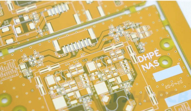
Of course, in HDI boards, we usually need blind buried vias.
Usually, the size of our blind vias ranges from 4/10±2, so that it can usually hit the pad, but it should be noted that it should not hit the center of the pad. It can usually hit the edge of the pad, which will be better in terms of process processing.
So is it better for our vias to be bigger or smaller? Obviously not.
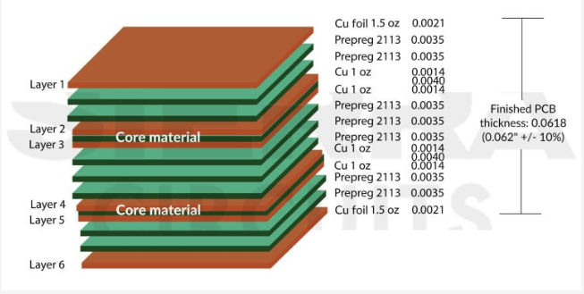
From a process point of view, the inner diameter of our vias cannot be less than 1/7 of the board thickness. Why?
Because when our vias are less than 1/7, due to the influence of process technology, we cannot evenly plate copper on the via hole wall. When we cannot evenly plate copper, the electrical performance of our board will be affected. Therefore, when the board thickness is larger, we should also increase the vias.
Our conclusion above is that it is better to go through a larger hole. At this point, we need to introduce two formulas to you. One is the calculation formula of via parasitic capacitance: C=1.41εTD2/(D1-D The other is the calculation formula of parasitic inductance: L=5.08h[ln(4h/d)+1].
First, let’s take a look at the calculation formula of via parasitic capacitance:
ε: dielectric constant of the board, usually the dielectric constant of different boards is also different, T: refers to the thickness of the board.
Assuming that the via is GND, in this case, the D1 value is the avoidance distance between the edge of the via and the copper skin (anti-pad), and D2: refers to the outer diameter of the via.
We can draw conclusions from the above formulas:
- When the board and board thickness remain unchanged, the larger the parasitic capacitance of D, the smaller the parasitic capacitance, and C is inversely proportional to D1.
- When the board and thickness remain unchanged, the larger the parasitic capacitance of D, the larger the parasitic capacitance, and C is proportional to D2.
- When the board thickness and D2, D remain unchanged, the larger the dielectric constant of the board, the larger the parasitic capacitance, and C is proportional to ε.
- The larger the dielectric constant and D2,D, the greater the board thickness T, the greater the parasitic capacitance.
In ordinary PCB design, the parasitic capacitance and parasitic inductance of vias have little effect on PCB design, and conventional selection can be made. However, at high speed. Through the analysis of the above-mentioned via parasitic characteristics, we can see that the intermediate via design is in high-speed PCB design. The seemingly simple vias often have a huge negative impact on the circuit design
.
In order to reduce the adverse effects of via parasitic effects, the following can be done as much as possible in the design:
1) Choose a reasonable via size. For multi-layer general density PCB design, it is better to choose 10/20/36 POWER isolation area) vias; for vias of power or ground wires, consider using a larger size to reduce impedance;
2) The larger the POWER isolation area, the better;
3) PCB signal routing should not change layers as much as possible, that is, minimize vias;
4) Using thinner PCBs, the two parasitic parameters are conducive to reducing vias;
Of course, specific problems need to be analyzed in the design. Considering the cost and signal quality, when designing PCB at high speed, designers always hope that the holes are as small as possible, so that the wiring space on the board is larger. In addition, the smaller the hole, the smaller its own parasitic capacitance, which is more suitable for high-speed circuits.
In high-density PCB design, the reduction of non-vias (blind buried vias) and via sizes has increased costs. The via size cannot be reduced infinitely, which affects PCB manufacturers to limit drilling and plating and other process technologies at high speed. PCB via design should consider balance.
Then, after understanding the above information, we will know why we can’t punch too many vias in high-speed PCB design. Vias themselves will bring parasitic capacitance and parasitic inductance. The more vias, the greater the value of parasitic capacitance and parasitic inductance. So this is why many data manuals will write that the number of vias cannot exceed a certain number when we are wiring. Generally, our high-speed signal lines adopt the principle of no more than three vias, and we don’t punch holes if we can.