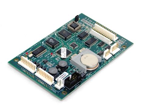
Why do circuit boards need copper cladding?
Generally, there are several reasons for copper cladding.
1.EMC. For large-area ground or power copper cladding
It will play a shielding role. Some special grounds, such as PGND, play a protective role.
2.PCB process requirements.
Generally, in order to ensure the electroplating effect or lamination deformation, copper is laid on PCB layers with less wiring.
3.Signal integrity requirements
give high-frequency digital signals a complete return path, and reduce the wiring of the DC network. Of course, there are also heat dissipation, special device installation requirements and other reasons.
4.One of the great benefits of copper cladding is to reduce ground impedance (the so-called anti-interference is also largely caused by the reduction of ground impedance).
There are a lot of spike pulse currents in digital circuits, so it is more necessary to reduce ground impedance. It is generally believed that for circuits composed entirely of digital devices, large areas should be laid, while for analog circuits, the ground loop formed by copper cladding will cause electromagnetic coupling interference, which is not worth the loss (except for high-frequency circuits). Therefore, not every circuit needs to be copper clad (BTW: mesh copper cladding has better performance than whole-block cladding).
5.The significance of copper plating in circuits
6.Copper plating is connected to the ground wire, which can reduce the loop area.
7.Large-area copper plating is equivalent to reducing the resistance of the ground wire and reducing the voltage drop.
From these two points of view, whether it is digital ground or analog ground, copper plating should be used to increase the anti-interference ability, and at high frequencies, the digital ground and analog ground should be separated and copper plating should be used, and then connected with a single point. The single point can be wound around a magnetic ring with a wire for several turns and then connected. However, if the frequency is not too high, or the working conditions of the instrument are not bad, it can be relatively relaxed. The crystal oscillator can be regarded as a high-frequency emission source in the circuit. You can plating copper around it and then grounding the shell of the crystal oscillator, which will be better.

8.What is the difference between the whole block of copper plating and the grid?
Let’s analyze it specifically.
There are about 3 functions:
1. Beautiful
2. Suppress noise
3. In order to reduce high-frequency interference (reasons on the circuit board) According to the routing principle: the power supply and the ground layer should be as wide as possible.
Why do we need to add a grid?
Isn’t it inconsistent with the principle? If we look at it from the perspective of high frequency, it is even more wrong. The most taboo in high-frequency wiring is sharp routing. There are many problems if there are many 90-degree lines on the power layer. In fact, the reason why it is done in that way is completely due to the requirements of the process: see if there is such a drawing for manual soldering, almost no; if you see such a drawing, there must be a surface-mount chip on it. At that time, there is a process called wave soldering when mounting chips. It needs to heat the board locally. If the copper is fully laid, the specific heat coefficients of the two sides are different, and the board will be warped. Once the board is warped, problems will arise. When putting on the steel cover (also a process requirement), it is easy to make mistakes on the chip pins, and the scrap rate will rise straight up. In fact, this approach also has disadvantages: under our current corrosion process: the film is easy to stick to it. In this case, in the subsequent strong acid process, that point may not be corroded, and there will be a lot of scraps. But if there is only, only the board is broken and the chip on it is ruined together with the board! From this perspective, do you understand why it is drawn like that? Of course, some surface mount products do not have a grid. From the perspective of product consistency
There may be two situations:
1. Its corrosion process is very good;
2. It does not use wave soldering but uses a more advanced reflow soldering. However, in this case, the investment in the entire assembly line will increase by 3-5 times.


