Why Do PCBs Warp? Understanding the Causes and Consequences
Introduction
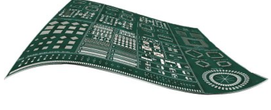
Printed Circuit Boards (PCBs) serve as the foundational platform for mounting and interconnecting electronic components in virtually all modern electronic devices. These thin, flat boards are designed to provide stable mechanical support and reliable electrical connections. However, one of the most common and problematic issues in PCB manufacturing and assembly is board warping or deformation. PCB warping refers to any undesired bending, twisting, or dimensional distortion of the board from its intended flat shape.
This phenomenon affects boards of all sizes, from small consumer electronics to large industrial control systems. Even minor warping can have significant consequences for product quality, reliability, and manufacturing yield. Understanding the root causes of PCB deformation and its potential impacts is crucial for designers, manufacturers, and quality control professionals in the electronics industry.
This article examines the primary causes of PCB warping, explores its various forms, and details the significant harms it can cause throughout the product lifecycle—from manufacturing to end-use operation.
Causes of PCB Warping
1. Material Selection and Properties
The choice of base materials fundamentally influences a PCB’s susceptibility to warping:
Coefficient of Thermal Expansion (CTE) Mismatch: The different layers in a PCB (copper, substrate, prepreg) expand and contract at different rates when subjected to temperature changes. Copper has a CTE of about 17 ppm/°C, while FR-4 substrate is typically 12-16 ppm/°C in the X-Y plane but 50-70 ppm/°C in the Z-axis. This mismatch creates internal stresses that can lead to warping.
Material Asymmetry: Uneven distribution of copper across the board layers creates an imbalance in mechanical stresses. For example, a board with dense copper routing on one side and sparse copper on the opposite side is prone to bending toward the less dense side.
Moisture Absorption: Many PCB substrate materials (especially older FR-4 formulations) absorb moisture from the environment. When this moisture turns to steam during high-temperature processes like reflow soldering, it can cause localized swelling and deformation.
2. Design Factors
Uneven Copper Distribution: As mentioned earlier, non-uniform copper coverage across layers creates mechanical stress imbalances. Designers should aim for symmetrical copper distribution, typically keeping density differences between opposite layers below 30%.
Layer Stackup Configuration: Improper layer sequencing or unbalanced stackup (odd number of layers with asymmetrical arrangement) can induce warping. Best practice is to use symmetrical stackups with even layer counts whenever possible.
Board Geometry: Large, thin boards are particularly susceptible to warping. The aspect ratio (length to thickness) significantly impacts warping risk—boards thinner than 1.6mm with dimensions over 150mm require special consideration.
3. Manufacturing Processes
Lamination Process: During PCB fabrication, the lamination process subjects the board to high temperature (typically 180-220°C) and pressure to bond layers together. Improper lamination parameters or uneven cooling can lock in residual stresses that later manifest as warping.
Thermal Cycling: Multiple heating and cooling cycles during manufacturing (drilling, plating, solder mask application) can accumulate thermal stresses in the board structure.
Mechanical Stress: Handling during manufacturing, especially for thin or large boards, can induce mechanical stresses that contribute to warping.
4. Assembly Processes
Reflow Soldering: The high temperatures (typically 220-260°C) of reflow soldering can exacerbate existing stresses or create new ones, particularly when different materials in the PCB assembly have mismatched thermal expansion properties.
Wave Soldering: While less common for surface-mount components, wave soldering can cause localized heating that leads to warping, especially for single-sided boards or those with significant copper imbalance.
Component Placement: Heavy components or asymmetric component distribution can create mechanical stress that contributes to warping, particularly when combined with thermal stresses during operation.
5. Environmental Factors
Temperature Variations: Operational temperature cycling in the field can cause progressive warping over time as materials expand and contract at different rates.
Humidity: Moisture absorption and release cycles can cause dimensional changes in the substrate material, potentially leading to warping.
Mechanical Loading: External forces during assembly, testing, or end-use can induce or exacerbate warping.
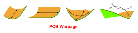
Types of PCB Deformation
PCB warping manifests in several distinct forms:
- Bow: A simple curvature where the board bends like a shallow “U” shape, with all four corners remaining in the same plane.
- Twist: A more complex deformation where one corner of the board is not coplanar with the other three, creating a twisted shape.
- Localized Warping: Deformation confined to specific areas of the board, often near cutouts, heavy components, or regions with significant copper density variations.
- Edge Lift: Where the edges of the board curl up or down while the center remains relatively flat.
Harms and Consequences of PCB Warping
1. Manufacturing and Assembly Issues
Solder Joint Defects: Warped boards can lead to various soldering problems during assembly:
- Non-wetting: Components may not make proper contact with solder paste
- Tombstoning: Chip components may stand up on one end due to uneven heating
- Bridging: Solder bridges may form between adjacent pads
- Head-in-pillow: BGA balls may not properly merge with solder paste
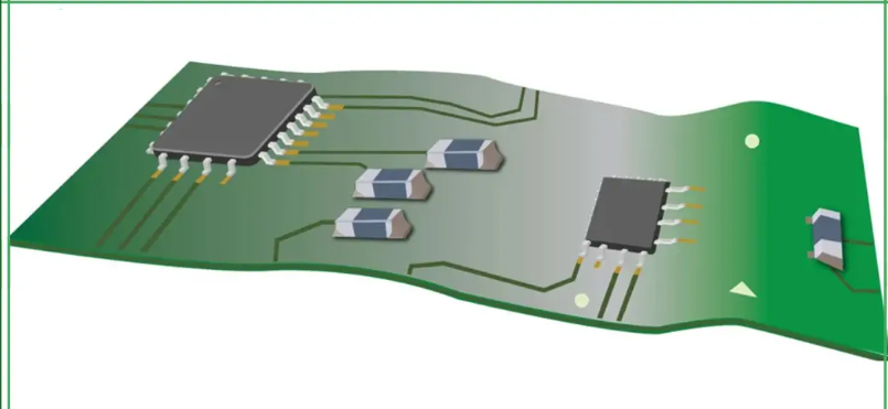
Pick-and-Place Problems: Automated assembly equipment relies on boards being flat for accurate component placement. Warping can cause:
- Misaligned components
- Placement accuracy issues
- Nozzle crashes in extreme cases
Fixture Incompatibility: Warped boards may not fit properly in test fixtures, assembly jigs, or final product enclosures.
2. Reliability Concerns
Mechanical Stress on Components: A warped board places continuous mechanical stress on mounted components, potentially leading to:
- Cracked components or packages
- Broken wire bonds in ICs
- Solder joint fatigue and eventual failure
Intermittent Connections: Flexing during operation can cause:
- Intermittent opens in traces or vias
- Contact problems in connectors
- Signal integrity issues in high-speed circuits
Delamination Risk: Severe or repeated warping can cause separation between PCB layers, particularly at high-stress points like via barrels.
3. Electrical Performance Impacts
Impedance Variations: For high-frequency circuits, warping changes the dielectric spacing and can alter controlled impedance traces, affecting signal integrity.
Current Carrying Capacity: Deformation may stress copper traces, potentially leading to increased resistance or complete opens in severe cases.
EMI Issues: Changed spacing between board layers or components can affect electromagnetic compatibility performance.
4. Operational and Safety Problems
Heat Dissipation Issues: Warping can create air gaps between the board and heatsinks or chassis, reducing thermal performance and potentially leading to overheating.
Mechanical Interference: In final products, a warped board may:
- Short against enclosure or other components
- Prevent proper closure of housings
- Interfere with moving parts
User Safety Concerns: In extreme cases, warping-related failures could lead to safety hazards like overheating or electrical shorts.
5. Quality and Cost Impacts
Reduced Yield: Warping-related defects directly impact manufacturing yield, increasing costs.
Rework Requirements: Warped boards often require manual intervention or rework, adding labor costs.
Field Failures: Latent warping-related issues may manifest after product shipment, leading to warranty claims and reputation damage.
Conclusion
PCB warping is a multifaceted issue stemming from material properties, design decisions, manufacturing processes, and environmental factors. Its consequences range from immediate manufacturing defects to long-term reliability problems that can significantly impact product quality and lifecycle costs.
Mitigating PCB warping requires a holistic approach encompassing:
- Careful material selection
- Balanced board design
- Controlled manufacturing processes
- Proper handling throughout the product lifecycle
By understanding the root causes and potential harms of PCB deformation, engineers and manufacturers can implement appropriate prevention strategies and quality controls. In an era of increasingly dense and miniaturized electronics, where tolerances continue to shrink, managing PCB warping remains a critical challenge for the electronics industry.
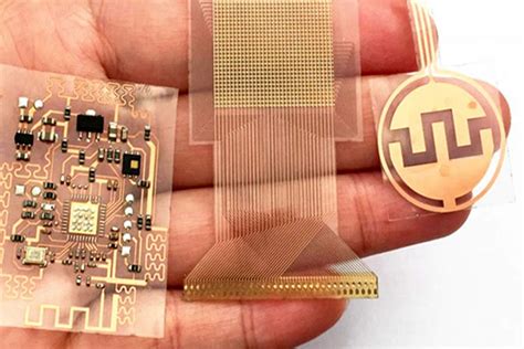
Future developments in PCB materials, manufacturing techniques, and design tools will continue to address warping challenges, particularly as the industry moves toward flexible and rigid-flex solutions that intentionally incorporate controlled deformation as part of their functionality. However, for conventional rigid PCBs, maintaining flatness remains an essential requirement for quality and reliability.