Why Immersion Gold and Gold Plating are Used on PCB Boards
Introduction
Printed Circuit Boards (PCBs) form the backbone of modern electronics, providing the physical platform to mount and interconnect electronic components. Among the various surface finishing techniques applied to PCBs, immersion gold (ENIG – Electroless Nickel Immersion Gold) and gold plating (electrolytic gold) have become two of the most important and widely used processes in PCB manufacturing. This 2000-word article explores the technical reasons behind using these gold-based surface finishes, their comparative advantages, and their specific applications in different electronic products.
1. The Fundamental Need for PCB Surface Finishing
Before examining gold-based finishes specifically, it’s essential to understand why PCB surfaces require special treatment at all:
1.1 Protection Against Oxidation
Copper, the primary conductive material in PCBs, oxidizes readily when exposed to air. This copper oxide layer forms quickly and significantly degrades solderability. Surface finishes prevent this oxidation, maintaining good electrical connectivity.
1.2 Enhancing Solderability
A proper surface finish ensures reliable solder joints during component assembly. Poor solderability leads to defective connections that compromise product reliability.
1.3 Providing a Contact Surface
For connectors and contact points, the surface finish must maintain low contact resistance through repeated mating cycles and environmental exposure.
1.4 Wire Bonding Compatibility
Many advanced packages require wire bonding directly to the PCB, necessitating surfaces suitable for gold or aluminum wire bonding.
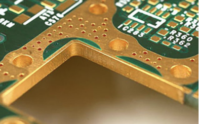
2. Immersion Gold (ENIG) Process and Advantages
Immersion gold, more accurately called Electroless Nickel Immersion Gold (ENIG), involves two main deposition layers:
2.1 Process Overview
- Electroless Nickel Deposition: A 3-6 μm layer of nickel-phosphorus alloy is chemically deposited on the copper surface.
- Immersion Gold Plating: A thin 0.05-0.1 μm gold layer displaces nickel atoms at the surface through an immersion reaction.
2.2 Key Advantages
Flat Surface: ENIG provides an exceptionally flat surface, critical for fine-pitch components and modern packaging technologies like BGA (Ball Grid Array).
Oxidation Resistance: The gold layer completely seals the surface from oxidation, offering long-term shelf life (typically 12 months or more).
Wire Bondability: The nickel-gold combination supports both gold and aluminum wire bonding, making it ideal for hybrid circuits.
Lead-Free Compatibility: ENIG performs well with lead-free soldering processes requiring higher temperatures.
Consistent Thickness: As a chemical process, ENIG produces very uniform thickness even on complex geometries.
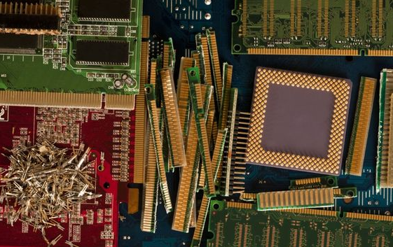
3. Electrolytic Gold Plating Characteristics
Electrolytic gold plating differs significantly from immersion gold in process and application:
3.1 Process Description
- Initial Layer: Often starts with a nickel undercoat similar to ENIG.
- Electroplating: Uses electrical current to deposit gold, allowing much thicker deposits (typically 0.5-2.5 μm).
3.2 Primary Benefits
Durable Contacts: Thicker gold withstands repeated insertion cycles in connectors and contact points.
Custom Thickness: Different areas can receive different gold thicknesses through selective masking.
Pure Gold Options: Electroplating can deposit hard gold (alloyed with cobalt or nickel) for wear resistance or soft pure gold for optimal conductivity.
4. Comparative Analysis: Immersion Gold vs. Gold Plating
4.1 Thickness Considerations
- Immersion Gold: Limited to about 0.1 μm maximum due to the self-limiting nature of the displacement reaction.
- Gold Plating: Can achieve much greater thicknesses (1-50 μm or more) for demanding applications.
4.2 Cost Factors
- Immersion Gold: Generally more cost-effective for standard applications due to thinner gold usage.
- Gold Plating: Higher cost but justified for connectors and high-reliability applications.
4.3 Application Suitability
| Application | Preferred Finish | Reason |
|---|---|---|
| Fine-pitch components | Immersion Gold | Excellent flatness |
| Connectors | Hard Gold Plating | Wear resistance |
| Wire bonding | Immersion Gold | Reliable bond formation |
| High-frequency circuits | Immersion Gold | Consistent skin effect |
| Keyboard contacts | Hard Gold Plating | Withstands millions of cycles |
5. Technical Challenges and Solutions
5.1 Black Pad Syndrome (ENIG)
A potential failure mode where excessive phosphorus in the nickel layer causes brittle solder joints. Modern process controls including:
- Tight phosphorus content control (7-9%)
- Proper bath maintenance
- Intermediate cleaning steps
5.2 Porosity in Thin Gold Layers
For immersion gold, the thin layer may develop micro-porosity. Solutions include:
- Maintaining minimum 0.05 μm thickness
- Ensuring proper nickel surface preparation
- Using immersion gold with slight organic additives to improve density
5.3 Galvanic Corrosion Risks
The nickel-gold-copper sandwich creates galvanic potential. Mitigation involves:
- Complete gold coverage
- Avoiding exposure to ionic contaminants
- Conformal coating in harsh environments
6. Specialized Applications Requiring Gold Finishes
6.1 High-Reliability Electronics
Military, aerospace, and medical PCBs often specify gold finishes because:
- Long-term storage capability
- Resistance to fungal growth
- Stable contact resistance
6.2 RF and Microwave Circuits
Gold’s excellent conductivity and consistent thickness help maintain controlled impedance in high-frequency designs.
6.3 Harsh Environment Electronics
Automotive, industrial, and outdoor electronics benefit from gold’s:
- Corrosion resistance
- Temperature stability
- Chemical inertness
7. Alternative Surface Finishes and When Gold is Preferred
While HASL (Hot Air Solder Leveling), OSP (Organic Solderability Preservative), and immersion silver/tin exist, gold finishes are preferred when:
- Long shelf life is required (gold doesn’t tarnish)
- Fine features demand flat surfaces (ENIG is exceptionally planar)
- Wire bonding is needed (gold or aluminum wires bond best to gold)
- High reliability is critical (gold maintains stable contact resistance)
8. Cost-Benefit Analysis of Gold Finishes
Despite higher material costs, gold finishes often prove economical when considering:
- Reduced assembly defects: Fewer solder joint issues
- Longer product life: Especially for connectors and contacts
- Lower field failures: Critical for high-reliability applications
- Miniaturization enablement: Essential for modern high-density designs
9. Future Trends in Gold-Based PCB Finishes
9.1 Thinner but More Effective Layers
Advances in deposition technology allow:
- Sub-micron gold layers with improved porosity control
- Nanocomposite gold coatings for enhanced wear resistance
9.2 Selective Application Techniques
Laser-assisted and inkjet-based gold deposition enable:
- Precise gold application only where needed
- Reduced gold consumption
- Mixed finishes on single boards
9.3 Environmentally Friendly Processes
Development of:
- Reduced gold bath toxicity
- Improved recycling of gold from processing waste
- Alternative alloys for less critical applications
Conclusion
The use of immersion gold and gold plating on PCBs addresses fundamental requirements of modern electronics: reliability, performance, and miniaturization. While alternative finishes exist for cost-sensitive applications, gold-based finishes remain indispensable for high-performance and high-reliability electronics. The choice between immersion gold and gold plating depends on specific application requirements including wear resistance, solderability, wire bonding needs, and contact reliability. As electronic devices continue advancing, gold-based PCB finishes will maintain their critical role in enabling next-generation technologies while evolving to meet new environmental and economic challenges.