Why PCB Design Needs 3D Capabilities: A Comprehensive Analysis
Introduction
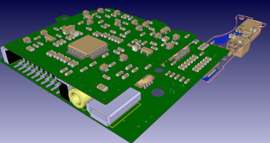
In the rapidly evolving world of electronics design, Printed Circuit Board (PCB) design has undergone a significant transformation from purely 2D layouts to sophisticated 3D modeling environments. This shift represents more than just a technological trend—it has become an essential requirement for modern electronics development. As electronic devices continue to shrink in size while increasing in complexity, the traditional 2D design approach can no longer adequately address the challenges faced by PCB designers and engineers.
This article explores the critical reasons why 3D functionality has become indispensable in PCB design. We will examine how 3D capabilities enhance mechanical integration, improve design accuracy, facilitate thermal management, support advanced manufacturing processes, and ultimately lead to better products with reduced development time and costs.
1. Mechanical Integration and Enclosure Compatibility
1.1 The Growing Importance of Form Factor
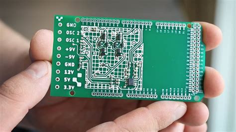
In today’s competitive electronics market, product aesthetics and ergonomics play a crucial role in consumer acceptance. The sleek smartphones, wearable devices, and IoT products that dominate the market require precise mechanical integration where every millimeter counts. 3D PCB design allows engineers to visualize and verify how the board fits within its enclosure long before physical prototyping begins.
1.2 Collision Detection and Component Placement
With 3D capabilities, designers can:
- Detect collisions between components and mechanical parts
- Verify clearances for connectors, cables, and mounting hardware
- Optimize component placement considering height restrictions
- Visualize the board assembly process
This proactive approach prevents costly redesigns that would otherwise be discovered only during physical assembly.
1.3 Integration with Mechanical CAD Systems
Modern 3D PCB tools offer seamless integration with mechanical CAD (MCAD) systems through standardized file formats like STEP or direct software integrations. This bi-directional communication enables:
- Real-time collaboration between electrical and mechanical teams
- Synchronized updates between PCB and enclosure designs
- Accurate representation of the complete product assembly
2. Enhanced Design Accuracy and Error Reduction
2.1 Beyond the Limitations of 2D
Traditional 2D design views present several limitations:
- Difficulty visualizing component heights and board stacking
- Challenges in assessing true spatial relationships
- Limited ability to predict manufacturing issues
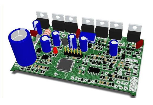
3D visualization overcomes these limitations by providing a more natural representation of the physical board.
2.2 Comprehensive Design Rule Checking (DRC)
While 2D DRC checks electrical spacing rules, 3D DRC extends this verification to:
- Component-to-component mechanical interference
- Board-to-enclosure clearances
- Keepout zone violations in three dimensions
- Connector mating alignment
2.3 Improved Manufacturing Preparation
3D visualization helps identify potential manufacturing issues such as:
- Solder mask clearance problems
- Component shadowing during reflow soldering
- Wave soldering interference
- Automated optical inspection (AOI) challenges
3. Thermal Management and Performance Optimization
3.1 Visualizing Thermal Profiles
Modern high-density designs generate significant heat that must be properly managed. 3D PCB tools enable:
- Visualization of component heat distribution
- Simulation of airflow paths
- Identification of thermal hotspots
- Planning for heat sink placement and thermal vias
3.2 EMI/EMC Considerations
3D electromagnetic simulation capabilities help designers:
- Predict and mitigate electromagnetic interference
- Optimize shielding requirements
- Visualize current density distributions
- Plan grounding strategies more effectively
3.3 Signal Integrity in Three Dimensions
High-speed designs benefit from 3D analysis of:
- Via stub effects
- Differential pair routing in multilayer boards
- Crosstalk between adjacent layers
- Impedance matching in complex geometries
4. Support for Advanced Manufacturing Technologies
4.1 Flexible and Rigid-Flex PCBs
The growing adoption of flexible circuits demands 3D visualization to:
- Simulate bend radii and folding patterns
- Analyze stress points in dynamic flex applications
- Verify component placement in relation to bend areas
- Plan stiffener placement and material transitions
4.2 Embedded Components
3D design tools are essential for:
- Visualizing cavities for embedded passives and actives
- Planning laser drilling and milling processes
- Verifying depth relationships in the Z-axis
- Ensuring proper material buildup around embedded parts
4.3 3D Printed Electronics
As additive manufacturing enters PCB production, 3D design capabilities enable:
- Modeling of non-planar circuit geometries
- Integration of printed electronic components
- Design of conformal shielding and antennas
- Visualization of multilayer inkjet-printed circuits
5. Improved Collaboration and Communication
5.1 Cross-Disciplinary Understanding
3D models serve as a universal language that bridges gaps between:
- Electrical engineers and mechanical designers
- PCB designers and manufacturing engineers
- Design teams and management stakeholders
- Companies and their customers or suppliers
5.2 Enhanced Design Reviews
Interactive 3D models facilitate more productive design reviews by:
- Allowing rotation and section views for complete inspection
- Enabling markups and annotations directly on the 3D model
- Supporting virtual reality (VR) walkthroughs
- Providing clearer communication of design intent
5.3 Documentation and Manufacturing Handoff
3D capabilities improve manufacturing preparation through:
- Automated 3D PDF generation for documentation
- Interactive assembly instructions
- Clear visualization of special requirements
- Reduced ambiguity in manufacturing specifications
6. Future-Proofing PCB Design Practices
6.1 Supporting Emerging Technologies
3D design capabilities position companies to adopt:
- Heterogeneous integration and chiplets
- Advanced packaging technologies
- 3D IC stacking
- MEMS integration
6.2 Digital Twin Implementation
3D PCB models form the foundation for:
- Product lifecycle management (PLM) systems
- Digital twin simulations
- Virtual prototyping
- Augmented reality (AR) maintenance guides
6.3 Artificial Intelligence and Automation
3D-aware design systems enable:
- Machine learning for component placement optimization
- Automated routing considering 3D constraints
- Generative design for innovative solutions
- Predictive analysis of manufacturing outcomes
Conclusion
The integration of 3D capabilities into PCB design tools has transitioned from a luxury to an absolute necessity in modern electronics development. As products become more compact and complex, the ability to visualize, analyze, and validate designs in three dimensions significantly reduces risk, improves quality, and accelerates time-to-market.
From ensuring proper mechanical fitment to optimizing thermal performance, from enabling advanced manufacturing techniques to facilitating better collaboration, 3D PCB design addresses challenges that simply cannot be adequately handled in a 2D environment. Furthermore, as we look toward the future of electronics with technologies like flexible hybrid electronics, 3D IC integration, and additive manufacturing, the importance of 3D design capabilities will only continue to grow.
For companies looking to maintain competitiveness in the electronics industry, investing in and adopting 3D PCB design capabilities is not just an option—it’s an essential strategy for success in an increasingly complex and demanding technological landscape. The question is no longer whether PCB design needs 3D functionality, but rather how quickly organizations can fully implement and leverage these capabilities throughout their design and manufacturing processes.