Why PCB Design Tools Are Progressing So Slowly
Introduction
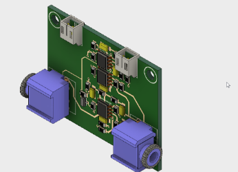
Printed Circuit Board (PCB) design tools form the backbone of electronics development, enabling engineers to transform conceptual schematics into physical layouts that can be manufactured. While the electronics industry has seen exponential growth and innovation over the past few decades, PCB design software has evolved at a comparatively glacial pace. This article examines the multifaceted reasons behind the slow progression of PCB design tools, exploring technical challenges, market dynamics, user resistance to change, and the complex nature of electronics design itself.
The Complexity of Modern PCB Design
One fundamental reason for slow progress lies in the ever-increasing complexity of PCB design itself. Modern circuit boards must accommodate:
- High-speed digital signals with frequencies exceeding 100GHz
- Mixed-signal designs combining analog, digital, and RF components
- Miniaturization trends leading to high-density interconnects (HDI)
- Thermal management challenges in compact designs
- Manufacturing constraints and design for excellence (DFX) requirements
Each new technological advancement in electronics creates additional requirements for PCB design tools. Rather than leading innovation, EDA (Electronic Design Automation) tools often play catch-up with emerging technologies. The software must maintain backward compatibility while adding support for new features—a balancing act that slows down fundamental architectural improvements.

Fragmented Ecosystem and Legacy Code
The PCB design software landscape suffers from decades of accumulated technical debt:
- Legacy codebases: Many commercial tools originated in the 1980s or 1990s, built on architectures that predate modern computing paradigms
- File format inertia: Industry-standard formats like Gerber (introduced in 1980) and Excellon drill files limit how radically tools can evolve
- Plugin dependencies: Many organizations rely on third-party plugins that may not support new features
- OS compatibility: Tools must maintain support for older operating systems used in some enterprises
One senior developer at a major EDA company revealed: “About 40% of our development effort goes into maintaining compatibility with workflows that should have been retired years ago. We can’t remove old features because some large customers have automated scripts that depend on them.”
Economic Factors and Market Dynamics
The business aspects of PCB tools create significant inertia:
- High switching costs: Companies invest heavily in training and design libraries tied to specific tools
- Oligopolistic market: A few major players dominate, reducing competitive pressure for innovation
- Niche market: Compared to general productivity software, PCB tools serve a relatively small professional audience
- Long sales cycles: Enterprise sales to large electronics companies move slowly
- Fragmented user needs: Hobbyists, startups, and multinational corporations have vastly different requirements
These factors create a market where incremental updates are safer than disruptive innovation. As noted by industry analyst Mark Greenfield: “EDA companies make more money selling maintenance contracts for stable tools than risking revolutionary changes that might alienate existing customers.”
User Resistance to Workflow Changes
PCB designers—often conservative in their tool preferences—frequently resist fundamental changes:
- Steep learning curves: Mastering PCB tools takes years, making designers reluctant to relearn
- Risk aversion: When product deadlines loom, designers stick with familiar tools
- Standardization needs: Large teams must use identical tools for collaboration
- Validation concerns: New tools require re-verification of design rules and outputs
A survey of 500 PCB designers found that 68% would only switch tools if their current solution became “completely inadequate” for their needs. This user conservatism removes much of the incentive for radical innovation.
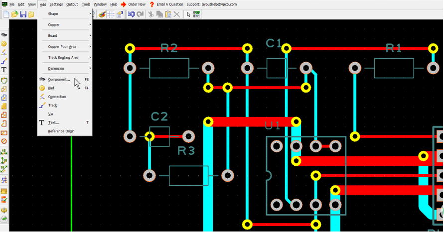
Integration Challenges in the EDA Ecosystem
Modern electronics design involves multiple specialized tools that must interoperate:
- Schematic capture
- PCB layout
- Signal integrity analysis
- Thermal simulation
- 3D mechanical CAD
- Version control systems
- Component management databases
Maintaining compatibility across this toolchain creates enormous complexity. Any fundamental change in one tool risks breaking integrations with others. As noted by Altium’s CTO: “We could redesign our UI to be much more modern, but then it wouldn’t match the look and feel of the simulation tools our customers also use.”
Verification and Reliability Requirements
Unlike consumer apps that can release “minimum viable products” and iterate quickly, PCB tools demand extreme reliability:
- Zero tolerance for errors: A bug could cause costly manufacturing mistakes
- Lengthy validation cycles: New versions undergo months of testing at customer sites
- Regulatory compliance: Some industries require tool qualification (e.g., aerospace, medical)
- Manufacturing handoff: Tools must produce perfectly accurate output files
These constraints naturally slow the release cycle. One validation engineer explained: “We test each new version against 5,000 historical designs to ensure nothing breaks. That process alone takes six weeks.”
The Specialized Talent Shortage
Developing PCB software requires rare expertise at the intersection of:
- Advanced software engineering
- Electrical engineering fundamentals
- Physics (for signal integrity, thermal modeling)
- Manufacturing processes
- User experience design
This combination is difficult to find, limiting the talent pool available to drive innovation. Universities rarely offer programs that cover all these areas, leaving companies to train developers extensively.
Attempts at Innovation and Their Challenges
Some companies have attempted to modernize PCB design tools with mixed success:
- Browser-based tools: Face performance limitations with complex designs
- AI-assisted routing: Struggles with the nuanced constraints of real-world designs
- Collaborative cloud platforms: Raise IP security concerns for many companies
- Simplified interfaces: Often lack the depth needed for professional designs
These efforts frequently encounter the same fundamental barriers: the complexity of electronics design and the conservative nature of the user base.
Promising Developments on the Horizon
Despite these challenges, several areas show potential for accelerating PCB tool innovation:
- Cloud computing: Enables more sophisticated simulation and analysis
- Machine learning: Could automate routine design tasks
- Standardization efforts: New formats like IPC-2581 may reduce legacy constraints
- Open-source initiatives: Projects like KiCad are introducing fresh approaches
- Generative design: Emerging techniques for automated topology optimization
However, widespread adoption of these innovations will require overcoming the same systemic barriers that have constrained progress thus far.
Conclusion
The slow evolution of PCB design tools stems from a perfect storm of technical debt, market dynamics, user conservatism, and the intrinsic complexity of modern electronics design. While frustrating for engineers eager for better tools, this gradual pace also reflects the mission-critical nature of PCB design—where reliability and precision must trump flashy innovation. Real progress will require coordinated efforts across the entire electronics ecosystem: EDA vendors addressing architectural legacy issues, manufacturers updating standards, companies modernizing their workflows, and educators preparing the next generation of tool developers. Until then, PCB design tools will likely continue their incremental evolution—slowly but steadily adapting to the changing landscape of electronics innovation.