Will the impedance mutation of a small section of the link affect the signal quality?
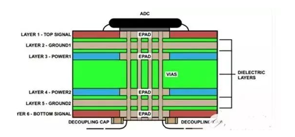
When designing PCB, I believe that experienced engineers have encountered this situation. During the wiring process, sometimes due to circuit structure or space limitations, a certain section of the line needs to be thicker or thinner, such as series resistors and capacitors, lower holes, BGA outlet areas or densely populated areas, etc., but the result of doing so is that the impedance of the signal line is discontinuous, and in severe cases it may even affect the quality of the signal.
So when faced with such a situation, how can we better control the design to avoid or reduce the impact on the signal quality?
This article will use SIGRITY simulation software to simulate and analyze the situation where a series line impedance mutation occurs on the signal transmission line, and understand how the series line impedance mutation affects the signal quality, so that we can easily complete the design when encountering similar impedance mutations in the design.
The simple simulation topology is shown in the figure below:
The internal resistance of the excitation source Vs is 50ohm, TL and TL2 are both 50ohm impedance, and the delay is 1ns.
The uniform transmission line, TL1 is used as a variable to simulate the line segment with impedance mutation during PCB wiring. The load resistor is a 100K resistor, which is equivalent to an open circuit termination.
In order to let us more intuitively understand the impact of the impedance mutation of the series trace in the transmission line on the signal, the simulation topology based on the above is set as follows:
The excitation source Vs is set to an ideal square wave with an amplitude of 1V;
TL1 is set to an impedance of 30ohm and a delay of 0.2ns;
Simulation results:
According to the simulation results, we can see that under the current model configuration, the signal level amplitude drops to 0.765V at the worst time, which has seriously affected the signal quality. In order to make it easier for everyone to understand the impact of this mutation on the signal, we can also use the reflection principle for calculation and analysis to see if it is consistent with our simulation results. The knowledge of reflection theory will not be elaborated here. Interested friends can pay attention to Mr. Gaoshou’s previous articles, which have detailed descriptions!
The analysis is as follows:
0ns:
The first reflection, the internal resistance of the excitation source is divided, and the voltage at point A is 0.5V;
1ns:
The second reflection, the boundary at point B, the reflection coefficient is -0.25, and the voltage on the TL1 transmission line is 0.375V;
1.2ns:
The third reflection, the boundary at point C, the reflection coefficient is 0.25, and the voltage on the TL2 transmission line is 0.46875V;
2.2ns:
The fourth reflection, the boundary at point D, the reflection coefficient is 1, and the load receives the voltage of 0.937V;
4.2ns:
The voltage reflected back by the load is reflected back at the boundary at point C. Affected by the reflection, the voltage received by the load at this time becomes 0.765V;
It can be seen that the simulation results are consistent with our calculation and analysis results.
Through the above simulation examples and analysis, I believe that everyone has a certain understanding of the principle of how the impedance mutation of the series routing in the transmission line affects the signal quality! Next, let’s simulate other impedance mutations to see if we can find some valuable rules. The simulation topology is also set as follows:
The excitation source Vs is set to an ideal square wave with an amplitude of 1V;
The impedance of TL1 is set to 30, 40, 50, 60, 70ohms, and the delay is 0.2ns;
Simulation results:
From the simulation results, we can see that the greater the impedance mutation of the series trace, the greater the impact on the signal quality. Therefore, when PCB wiring, it is necessary to ensure the continuity of the transmission line impedance or reduce the degree of impedance mutation as much as possible.
Of course, the above simulation studies are based on ideal square waves that do not exist in reality. Next, let’s take a look at what happens when the signal rise time is not 0? The simulation topology is also set as follows:
The excitation source Vs is set to a pulse with an amplitude of 1V and a rise time of RT=1ns;
TL1 is set to an impedance of 30ohm and a delay of 0.2ns;
Comparison of simulation results with ideal square wave simulation results:
According to the simulation results, when the signal rise time is 1ns, the worst signal level is 0.893V, and the signal quality is significantly improved compared to the 0.765V of the ideal square wave. Can it be considered that the impact of the impedance mutation of the series trace on the transmission line on the signal quality is related to the rising edge of the signal? Next, we will continue to do further simulation verification to observe whether there is a correlation between them. The simulation topology is also set as follows:
The excitation source Vs is set to 1V, and the rise time RT is set to 0.5ns, 1ns, and 1.5ns pulses respectively;
TL1 is set to 30ohm impedance and 0.2ns delay;
Simulation results:
The simulation results show that,
When RT=0.5ns, the worst signal level is 0.807V;
When RT=1.0ns, the worst signal level is 0.893V;
When RT=1.5ns, the worst signal level is 0.928V.
It can be seen that when the rise time of the signal is longer, the impact of the impedance mutation section of the series trace on the signal quality is smaller, and the signal quality is better.
Because the reflections at the boundaries before and after the impedance mutation section are equal in size and opposite in direction, they will cancel each other out after experiencing twice the mutation delay, but before the cancellation, the signal quality will be affected by the reflection within the two times delay.
Deterioration, but if the rise time of the signal is large enough, the impact can be weakened or even almost completely covered up.
However, in actual design, the rise time of our signal is basically fixed. In addition to reducing the impedance mutation, what other factors can help us improve the impact of the mutation line segment on the signal quality?
I believe everyone has guessed it! That is the length of our impedance mutation segment, that is, the delay size of the signal when it is transmitted in the impedance mutation segment.
Without further ado, let’s take a look at the simulation verification! The simulation topology settings based on the construction are as follows:
The excitation source Vs is set to a pulse with an amplitude of 1V and a rise time RT=1ns;
TL1 is set to 30ohm impedance, and the delays are 0.01ns, 0.1ns, 0.2n, and 0.3ns respectively;
Simulation results:
The simulation results show that,
When the delay = 0.01ns, the worst signal level is 0.994V;
When the delay = 0.1ns, the worst signal level is 0.946V;
When the delay = 0.2ns, the worst signal level is 0.893V;
When the delay = 0.3ns, the worst signal level is 0.848V.
It shows that the longer the impedance mutation section is, the greater the impact of the impedance mutation section of the series trace on the signal quality. When the mutation length is short enough, the impact can be ignored. This is the same principle as the longer the signal rise time is, the smaller the impact of the impedance mutation section of the series trace on the signal quality.
Finally, based on the above simulation results and analysis, we can make the following summary on the impact of the impedance mutation of the series trace on the signal quality:
(1) The larger the impedance mutation of the series trace is, the greater the impact on the signal quality. Therefore, when designing PCB wiring, our series trace impedance mutation should be as small as possible;
(2) The longer the signal rise time is, the smaller the impact of the impedance mutation section of the series trace on the signal quality, that is, the better the signal quality.
(3) The longer the impedance mutation section is, the greater the impact of the impedance mutation section of the series trace on the signal quality. When the mutation length is short enough, the impact can be ignored. Therefore, when designing wiring, we should control the impedance mutation section of the trace as short as possible. Of course, the specific length should also be evaluated in combination with the rise time of the corresponding signal.