Wiring design scheme for the power supply part of the PCB board
All electronic engineers must know that PCB design plays a very important role in design. Taking the power supply as an example, PCB design will directly affect the EMC performance, output noise, anti-interference ability, and even basic functions of the power supply.
Spacing
For high-voltage products, the line spacing must be considered. The spacing that can meet the corresponding safety requirements is of course the best, but in many cases, for products that do not require certification or cannot meet certification, the spacing is determined by experience.
How wide is the spacing? It is necessary to consider whether the production can ensure the cleanliness of the board surface, environmental humidity, other pollution, etc.
For AC input, even if the board surface can be kept clean and sealed, the drain-source voltage of the MOS tube is close to 600V, and less than 1mm is actually quite dangerous!
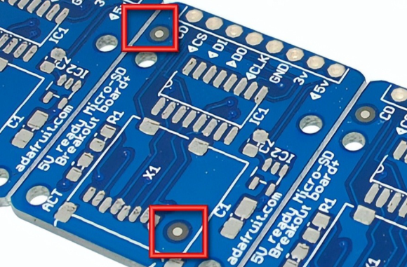
Components on the edge of the board
When placing chip capacitors or other easily damaged devices on the edge of the PCB, the PCB board direction must be considered. The figure shows the comparison of the stress magnitude of the device when various placement methods are used.

Figure 1 Comparison of stress on devices during board splitting
From this, it can be seen that the device should be far away from and parallel to the edge of the board splitting, otherwise the components may be damaged due to PCB board splitting.
Loop area
Whether it is input or output, power loop or signal loop, it should be as small as possible. The power loop emits electromagnetic field, which will lead to poor EMI characteristics or large output noise; at the same time, if it is received by the control loop, it is likely to cause abnormality.
On the other hand, if the power loop area is large, its equivalent parasitic inductance will also increase, which may increase the drain noise spike.
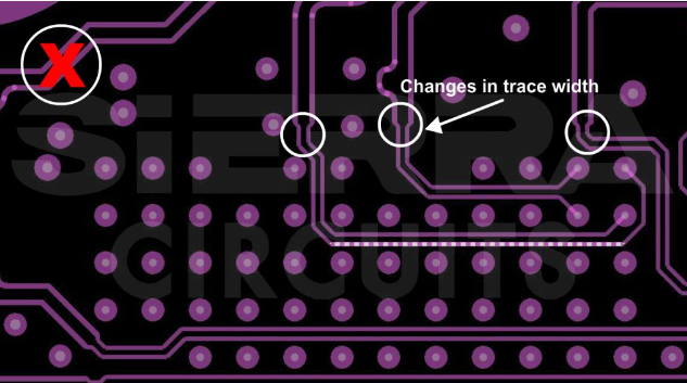
Critical routing
Due to the effect of di/dt, the inductance at the dynamic node must be reduced, otherwise a strong electromagnetic field will be generated. If the inductance is to be reduced, it is mainly necessary to reduce the length of the wiring, and increasing the width has little effect.
Signal line
For the entire control part, it should be considered to be away from the power part when wiring. If the two are close due to other restrictions, the control line should not be parallel to the power line, otherwise it may cause abnormal operation and oscillation of the power supply.
In addition, if the control line is very long, the pair of lines should be brought closer together, or placed on two surfaces of the PCB and facing each other, so as to reduce the loop area and avoid being interfered by the electromagnetic field of the power part. Figure 2 shows the correct and incorrect signal line routing methods between points A and B.
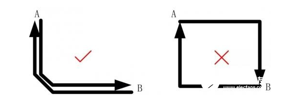
Figure 2 Correct and incorrect signal line routing methods.
Of course, the vias used for connection should be minimized on the signal line!
Copper plating
Sometimes copper plating is completely unnecessary and should even be avoided. If the copper area is large enough and its voltage is constantly changing, on the one hand it may act as an antenna to radiate electromagnetic waves to the surroundings; on the other hand it can easily pick up noise.
Usually only copper plating is allowed at static nodes, such as copper plating at the output “ground” node, which can equivalently increase the output capacitance and filter out some noise signals.
Mapping
For a loop, copper plating can be done on one side of the PCB, and it will automatically map according to the wiring on the other side of the PCB to minimize the impedance of this loop. This is like a group of impedances with different impedance values connected in parallel, and the current will automatically choose the path with the smallest impedance to flow through.
In fact, the control part of the circuit can be connected on one side, and copper can be laid on the “ground” node on the other side, and the two sides can be connected through vias.
Output rectifier diode
If the output rectifier diode is close to the output end, it should not be placed parallel to the output. Otherwise, the electromagnetic field generated at the diode will penetrate into the loop formed by the power output and the external load, increasing the measured output noise.
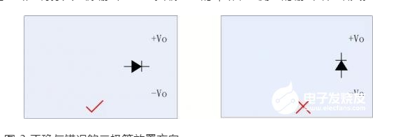
Figure 3 Correct and incorrect diode placement direction
Ground wire
The wiring of the ground wire must be very careful, otherwise it may cause EMS, EMI performance and other performance to deteriorate. For the “ground” of the switching power supply PCB, at least the following two points should be achieved:
The power ground and signal ground should be connected at a single point;
There should be no ground loop.
Y capacitor
The input and output are often connected to the Y capacitor. Sometimes, for some reasons, it may not be possible to hang it on the input capacitor ground. At this time, remember that it must be connected to a static node, such as the high-voltage end.
Others
When designing the actual power supply PCB, other issues may need to be considered, such as “the varistor should be close to the protected circuit”, “the common mode inductor should increase the discharge teeth”, “the chip VCC power supply should increase the ceramic capacitor”, etc. In addition, whether special treatment is required, such as copper foil, shielding, etc., also needs to be considered during the PCB design stage.
Sometimes there are often situations where multiple principles conflict with each other, and satisfying one of them cannot satisfy the others. This requires engineers to apply existing experience and determine the most appropriate wiring according to actual project requirements!
Summary
In order to create highly stable products, there are many design details required in hardware design. This article only introduces the most common power supply design in hardware. In order to make the overall product or system have stable and reliable power supply, most engineers will choose power modules as the basis for system power supply.
ZLG has nearly 20 years of industry experience in the isolated power modules independently developed and produced. At present, the products have a wide input voltage range, isolation 1000VDC, 1500VDC, 3000VDC and 6000VDC and other series, various packaging forms, compatible with international standard SIP, DIP and other packaging.
At the same time, ZLG has built a first-class test laboratory in the industry to ensure the performance of power products, equipped with the most advanced and complete test equipment. The full range of isolated DC-DC power supplies has passed the complete EMC test, with electrostatic immunity up to 4KV and surge immunity up to 2KV. It can be used in most complex and harsh industrial sites, providing users with stable and reliable power isolation solutions.