
0201 and 01005 Component Assembly: Challenges and Solutions
Modern consumer electronics demand higher functionality in smaller form factors, driving passive component dimensions to their physical limits. Research analyzing production data from over 500,000 boards shows that assembly lines working with 01005 components experience 4-6× higher defect rates than those handling standard 0402 packages—failures tied directly to placement accuracy, solder paste deposition, and reflow thermal profiles.
If you want to manufacture high-density PCBs for smartphones, wearables, or IoT devices with 0201 and 01005 components, you must understand ultra-fine-pitch assembly challenges, stencil aperture design, placement machine tolerances, tombstoning prevention strategies, and AOI verification methods. This technical guide provides proven solutions from production experience with miniature SMT assembly.
Understanding 0201 and 01005 Component Dimensions
0201 components measure 0.6mm × 0.3mm (metric 0603) with 0.3mm × 0.3mm pads. The 01005 package measures 0.4mm × 0.2mm (metric 0402) with 0.2mm × 0.2mm pads. These imperial designations derive from 20mil × 10mil and 10mil × 5mil dimensions.
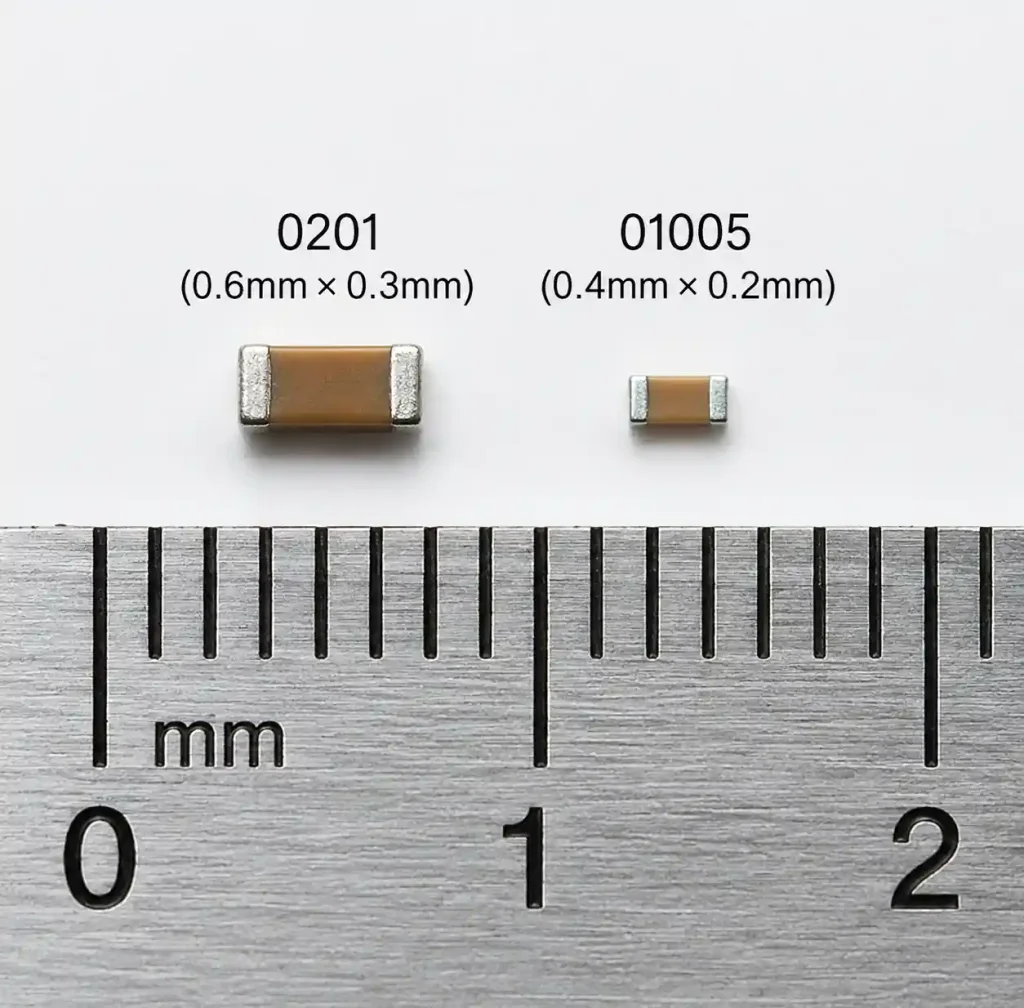
Component weight critically affects assembly reliability. A 0201 resistor weighs 0.2-0.4mg, while 01005 capacitors weigh 0.08-0.15mg. During reflow, surface tension forces exceed gravitational forces by 10-20×, causing susceptibility to tombstoning and displacement.
Critical Challenges in 0201 and 01005 Assembly
Ultra-miniature component assembly faces multiple technical hurdles that demand process optimization across every manufacturing stage.
| Challenge | 0201 Impact | 01005 Impact | Solution Approach |
|---|---|---|---|
| Placement Accuracy | ±50μm tolerance required | ±25μm tolerance required | High-precision placements with vision calibration |
| Solder Paste Printing | 0.3mm aperture minimum | 0.2mm aperture minimum | 75-100μm stencil thickness with electroformed foil |
| Tombstoning Risk | Moderate (3-5% defect rate) | High (6-12% defect rate) | Symmetric pad design and controlled ramp rates |
| AOI Detection | Difficult (requires 10μm resolution) | Extremely difficult (requires 5μm resolution) | X-ray inspection for hidden joints |
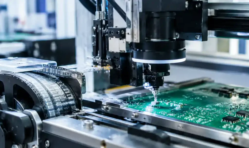
Placement machines must achieve sub-50μm accuracy for 0201 and sub-25μm for 01005 components. Standard pick-and-place systems calibrated for 0603 components cannot reliably handle these dimensions—vision systems struggle to distinguish component orientation when terminations measure just 100-150μm wide.
Stencil Design for Ultra-Fine-Pitch Components
Solder paste deposition determines assembly yield. Aperture design follows IPC-7525 area ratio requirements for proper paste release.
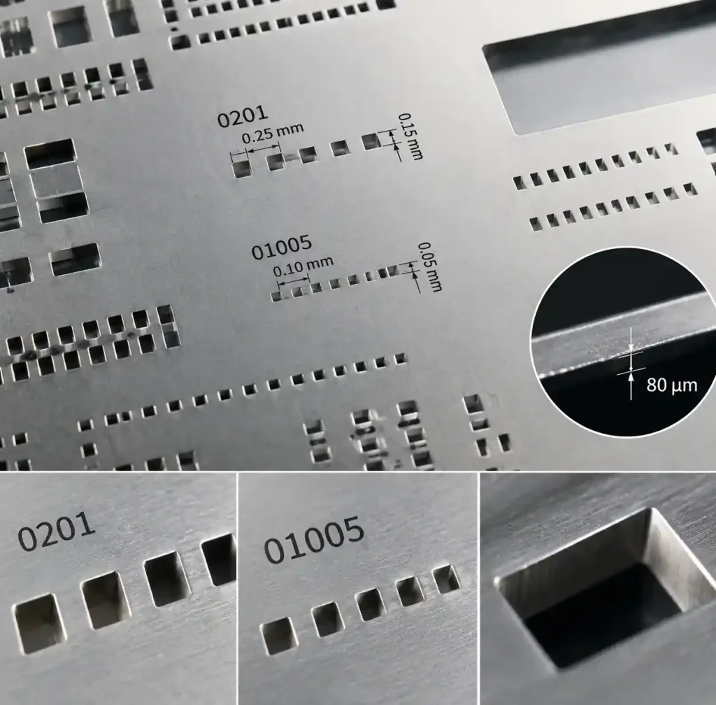
For 0201 components with 0.3mm pads, use 0.25mm × 0.25mm apertures with 100μm stencil thickness achieving 0.625 area ratio. For 01005, use 0.18mm × 0.15mm apertures with 75μm thickness for 0.6 area ratio—meeting the 0.55-0.66 target range.
Electroformed nickel stencils provide superior paste release versus laser-cut steel. Smooth, tapered walls improve transfer efficiency by 8-15% for sub-0.25mm apertures. Nano-coatings reduce bridging defects by 20-30%.
Placement Process Optimization Techniques
Placement force control is critical for components under 0.5mg. Excessive pressure deforms paste deposits; insufficient pressure causes poor adhesion.
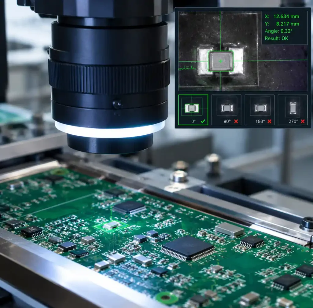
Optimal placement force: 50-80gf for 0201, 30-50gf for 01005. Vision systems verify orientation within ±1° and position within ±25μm. Angular errors exceeding 3° cause termination float, creating open circuits.
Use 0.2-0.3mm nozzles for 01005 and 0.4-0.5mm for 0201. Oversized nozzles lack vacuum pressure; undersized tips damage ceramic bodies. Clean nozzles every 2,000-5,000 placements.
Preventing Tombstoning in Miniature Components
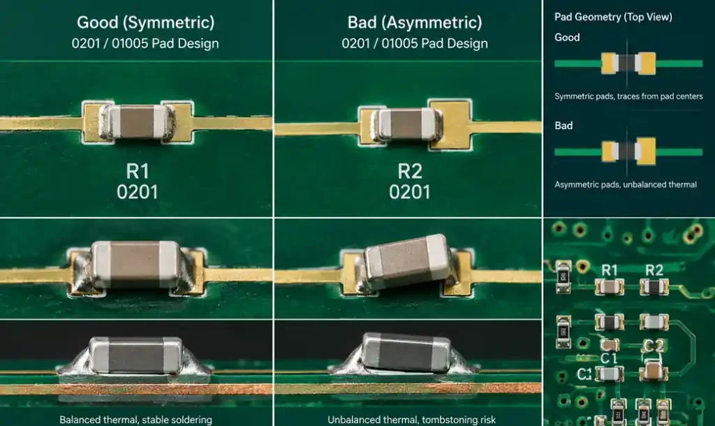
Tombstoning occurs when uneven heating or solder volume causes one component end to lift vertical during reflow. Light component weight and high surface tension make 0201 and 01005 packages especially vulnerable—field data shows tombstoning accounts for 35-45% of ultra-miniature component defects.
| Tombstoning Factor | Root Cause | Prevention Method |
|---|---|---|
| Asymmetric Heating | Temperature gradient >5°C between pads | Reduce ramp rate to 1-2°C/s in preheat zone |
| Uneven Solder Volume | Paste deposit variation >15% | Verify stencil aperture symmetry and printer alignment |
| Pad Design Imbalance | Unequal thermal mass or copper area | Match pad size within ±10% and route traces from pad centers |
| Component Weight | Parts <0.5mg susceptible to surface tension forces | Use SAC305 alloy with controlled wetting speed |
Symmetric pad geometry prevents thermal imbalance. Design both pads with identical dimensions (±5μm tolerance) and equal copper connection widths. Route traces from pad centers rather than edges to equalize heat transfer. For boards with large copper areas near one pad, add thermal relief patterns or dummy copper on the opposite side.
Reflow Profile Requirements for 01005 Components
Ultra-miniature components demand tighter thermal control. Rapid heating causes uneven wetting and tombstoning; insufficient peak temperature produces cold joints.
Optimal SAC305 profiles: 1.5-2.5°C/s preheat ramp (150-180°C soak for 60-90s) activates flux before melting. Reflow zone ramps 1-2°C/s to 235-245°C peak, held 30-60s above liquidus (217°C).
Cooling rate impacts joint formation—rapid cooling (>3°C/s) cracks ceramic bodies. Reduce to 2-3°C/s in first 50°C below peak. Nitrogen atmosphere improves wetting reliability by 12-18%.
AOI and X-Ray Inspection Strategies
Automated optical inspection faces significant challenges with ultra-miniature components. Standard AOI systems with 25-30μm resolution cannot reliably detect solder joint defects on 01005 packages where critical dimensions measure 150-200μm.
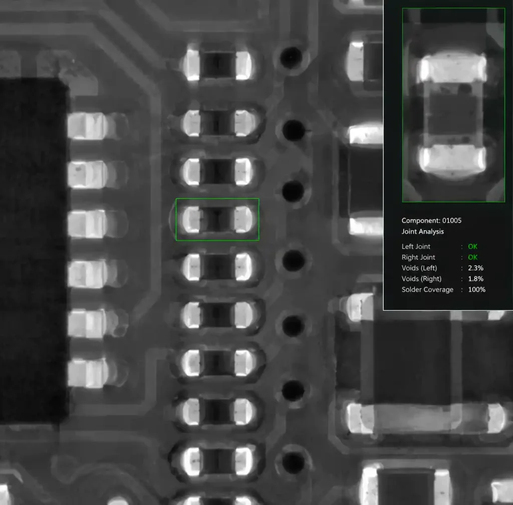
High-resolution AOI requires 10μm pixel resolution for 0201 and 5μm for 01005 verification. 3D solder paste inspection (SPI) before reflow catches 60-75% of potential defects by measuring paste height, volume, and position. Post-reflow AOI detects presence/absence, orientation, and visible joint quality, but cannot verify hidden joint integrity on ultra-small terminations.
X-ray inspection becomes mandatory for critical applications using 01005 components. 2D X-ray systems image solder joints through component bodies to verify wetting quality, void content, and termination contact. For complex assemblies, 3D X-ray or computed tomography (CT) provides void measurement accuracy within ±2% for joints as small as 0.15mm diameter. Learn more about PCB assembly inspection standards.
PCB Pad Design Guidelines
Land pattern design directly affects assembly yield. IPC-7351 provides nominal pad dimensions, but ultra-miniature components require tighter tolerances due to reduced process margins.
For 0201 components (0.6mm × 0.3mm body), specify 0.35mm × 0.35mm pads with 0.5mm center-to-center spacing. This provides 0.075mm toe extension, 0.025mm heel extension, and 0.15mm clearance between pads. NSMD (non-solder mask defined) pad construction improves solder wetting by allowing paste to flow onto pad sidewalls.
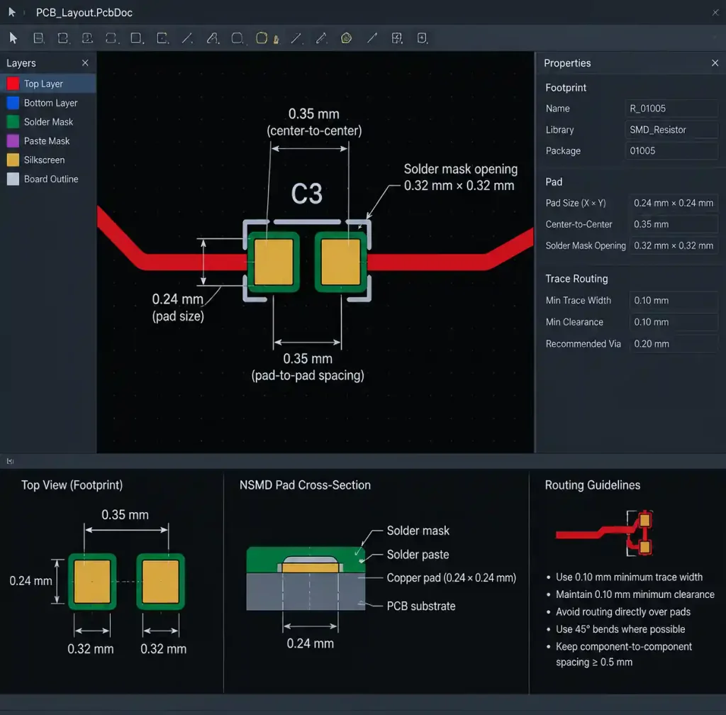
For 01005 components (0.4mm × 0.2mm body), reduce pads to 0.24mm × 0.24mm with 0.35mm spacing. Maintain minimum 0.05mm solder mask clearance around pads to prevent mask sliver defects. Solder mask dams between adjacent pads should measure ≥0.1mm to prevent bridging during reflow.
Route traces from pad centers at ≥0.075mm width for 0201 and ≥0.05mm for 01005 designs. Side connection traces create thermal asymmetry that increases tombstoning risk by 25-40%. When designing HDI PCB assemblies with ultra-miniature components, use microvias to escape routing without disturbing thermal balance.
Component Packaging and Handling Requirements
Tape and reel packaging uses 8mm tape with 0.8mm × 0.4mm pockets (0.3mm depth). Contamination causes vision failures and pick errors.
Store reels in moisture barrier bags (<10% RH). Ceramic components absorb moisture causing popcorning during reflow. Bake at 125°C for 24 hours if floor life expires.
Use precision feeders with 20-40gf tension control. Poor splice quality causes jams that damage terminations. Consider quick turn PCB assembly for prototypes.
Cost and Application Considerations
01005 component assembly costs 40-60% more than 0201 and 200-300% more than standard 0402 packages due to specialized equipment requirements, lower throughput, and higher defect rates. Total cost includes stencil tooling ($300-800 for electroformed nickel), placement machine upgrades ($50,000-150,000 for high-precision systems), and inspection equipment ($80,000-200,000 for high-resolution AOI or X-ray).
| Application | Component Size | Justification | Design Consideration |
|---|---|---|---|
| Smartphones | 01005 preferred | Space-critical: 15-20% density increase | RF filtering, power distribution |
| Wearables | 0201 / 01005 | Ultra-compact: <50mm² board area | Power management, sensor interface |
| IoT Sensors | 0201 common | Balance cost and density | Battery management, wireless frontend |
| Medical Implants | 01005 for critical paths | Miniaturization: <10mm device size | Long-term reliability requirements |
Use 01005 components only when board space constraints cannot be met with 0201 packages. Design analysis shows 0201 passives provide sufficient performance for most consumer applications while reducing assembly cost 35-50% and improving yield 8-12% compared to 01005 equivalents.
Frequently Asked Questions
What placement machine accuracy is required for 01005 assembly?
01005 assembly requires ±25μm placement accuracy. Standard SMT equipment calibrated for 0603 achieves ±50-75μm, insufficient for 01005 (0.4mm body). High-precision machines with dual-camera vision and closed-loop verification meet requirements with Cpk >1.33.
How does stencil thickness affect solder paste volume for 0201 components?
For 0201 (0.3mm pads), 100μm stencil deposits 0.009mm³ paste, providing 0.05-0.08mm fillet height. Thicker stencils (125-150μm) reduce transfer efficiency—area ratio drops below 0.5. Thinner stencils (75μm) improve release but limit solder volume.
What causes tombstoning in 01005 components?
Tombstoning results from differential wetting forces. Causes: uneven pad heating (>5°C gradient), unequal paste volume (>15% variation), asymmetric pad copper, excessive ramp rates (>3°C/s). Components <0.15mg face 15-25× surface tension versus gravity. Prevention: symmetric pads, controlled profiles, precise printing.
Can standard AOI detect defects on 01005 components?
Standard AOI (25-30μm resolution) cannot reliably detect defects on 0.15-0.20mm joints. High-resolution AOI (≤10μm) with 3D SPI verifies paste deposits. X-ray inspection provides best verification, imaging through bodies to detect wetting, voids, and contact quality.
What is the cost difference between 0201 and 01005 assembly?
01005 costs 40-60% more than 0201: electroformed stencils ($300-800 vs $150-300), placement upgrades ($50k-$150k), inspection equipment ($80k-$200k), longer setup (2-3×), lower yield (88-92% vs 95-98%). Below 10,000 units, premium exceeds 100%.
What PCB pad size for 01005 components?
IPC-7351 recommends 0.24mm × 0.24mm pads (0.12mm spacing). Use NSMD with mask opening 0.05-0.08mm larger. Maintain ±5μm symmetry and equal trace widths. Minimum 0.10mm solder mask dam prevents bridging.
Conclusion
Successful 0201 and 01005 component assembly requires integrated process control across stencil printing, placement accuracy, reflow thermal management, and advanced inspection techniques. Production data demonstrates that achieving 95%+ first-pass yield with these ultra-miniature packages demands placement accuracy within ±25μm, stencil apertures designed for 0.55-0.66 area ratio, symmetric pad geometry to prevent tombstoning, and reflow profiles with controlled 1-2°C/s ramp rates during liquidus transition.
For projects requiring ultra-high-density PCB assembly, Andwin Circuits offers precision SMT assembly capabilities for 0201 and 01005 components with advanced inspection including high-resolution AOI and X-ray verification. Our facility maintains ISO 9001 and IATF 16949 certification with proven experience in consumer electronics, medical devices, and IoT applications. We provide turnkey assembly services from prototype to production with fast turnaround in 7 days for quick-turn projects.
Contact us today for custom PCB assembly solutions with ultra-miniature components, complete DFM analysis, and competitive factory-direct pricing for your high-density electronic products.