10 Easy Steps to Design a PCB Circuit Board – Altium Designer
How to design a PCB board is not easy, but the right pcb design software can help a lot. Other engineers have spent some time learning the ropes of PCB design, and you can benefit from their experience. If you’re new to PCB design but still learning about designing custom circuit boards in Altium Designer®, we’ve compiled 10 important steps you can use to create a modern PCB layout for almost any application.
From basic printed circuits to complex non-rigid PCBs, there is a lot that goes into any engineering design. Any new electronic device will start with a block diagram and/or a set of electronic schematics. Once the schematic is completed and verified, you can follow the steps below to create a modern PCB layout in Altium Designer.
Here is a complete list of PCB layout and design steps:
1.Create schematic
2.Create a blank PCB layout
3.Schematic Capture: Link to Your PCB
4.Design PCB stackup
5.Define design rules and DFM requirements
6.Place component
7.Insert drill hole
8.route traces
9.Add tags and identifiers
10.Generate design files
GET PCB MANUFACTURING AND ASSEMBLY QUOTE NOW!
How to Design a Circuit Board in Ten Steps
When designing a circuit board, it sometimes seems like reaching the final design will be a long and arduous journey. Whether it’s the basics of microprocessing copper and solder, trying to make sure the board ends up printed, or having more specific design issues like through-hole technology or designing signals with vias, pads, and any number of layouts For completeness issues, you need to make sure you have the right design software.
If you’ve been doing this for decades, you don’t need me to tell you the value of knowing design software for properly designing printed boards. Without accurate and reliable integration from schematic capture to layout, laying out traces for wiring and copper or managing the layers required for solder can become difficult.
Despite being a deep program, Altium Designer’s user experience is very rewarding for both new and experienced PCB designers. It provides a new design environment that simplifies the custom circuit board design process in a unified PCB layout environment.
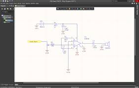
Step 1: Create Schematic
Whether you’re generating a design from a template or creating a printed circuit board from scratch, it’s always best to start with a schematic. A schematic is similar to a blueprint for a new device, so it’s important to understand what is shown in the schematic. First, the schematic shows you the following:
What components were used in the design
How components are connected together
Relationships between component groups in different schematics
The last point above is important because complex designs may use layered schematics. If you take a layered approach to your design and place different circuit blocks in different schematics, you can enhance important organization on your new board. You can learn more about the value of a well-designed schematic from Carl Schattke on the OnTrack Podcast.
Schematic Editor in Altium Designer
Not only are circuit interconnections easy to define and edit, but converting a schematic into a board layout is much easier than designing directly on the board. For components, Altium Designer has an extensive parts library database. Additionally, you can take advantage of Altium Vault, which provides access to thousands of component libraries and adds flexibility to your project management and product development. However, you can also design your own schematic symbols and create footprints. Or, if you’d like parts created for you, try Altium’s EE Concierge service.
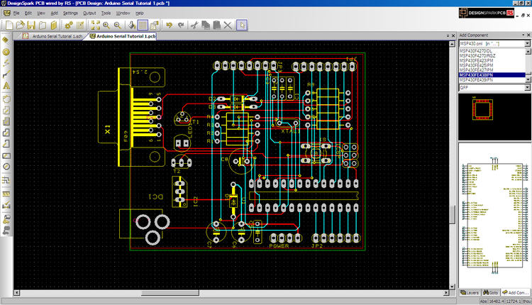
Step 2: Create a Blank PCB Layout
After creating the schematic, you need to use the schematic capture tool in Altium Designer to start creating the PCB layout. First, create a blank printed circuit board document, which will generate a PcbDoc file. This is done through Altium Designer’s main menu, as shown below.
Start a new PCB project in Altium Designer
If you have already determined the PCB shape, size and stackup of your board, you can set it up immediately. Don’t worry if you don’t want to perform these tasks now, you can change the board’s shape, size, and layer stacking later (see step 4 below). By compiling SchDoc, schematic information is available to PcbDoc. The compilation process includes validating the design and generating several project documents, allowing you to review and correct the design before transferring to PcbDoc, as shown below. It is strongly recommended that you check and update the project options used to create PcbDoc information at this time.
Project options for converting to PCB
Step 3: Schematic Capture: Link to PCB
All tools in Altium Designer are available in a unified design environment where schematics, PCB layouts and BOMs are related and accessible simultaneously. Other programs force you to manually compile schematic data, but Altium Designer does this for you automatically when creating your design. To transfer the SchDoc information to the newly created PcbDoc, click Design » Update PCB {File name of new PCB}.PcbDoc. The Engineering Change Order (ECO) dialog box opens, listing all components and nets in the schematic, similar to the following.
Engineering Change Order Example
Verify the changes by clicking the “Verify Changes” tab (SchDoc information is added to the project without errors). If the status of all items is green, click the Perform Changes tab. To complete the process, close the dialog box.
Step 4: Design PCB Stackup
When you transfer schematic information to PcbDoc, the component’s footprint is displayed in addition to the specified board outline. Before placing components, you should define the PCB layout (i.e. shape, layer stacking) using the Layer Stackup Manager as shown below.
If you are new to the world of printed circuit design, most modern PCB design concepts will start with a 4-layer board on FR4, although any number of layers can be defined in Altium Designer. You can also take advantage of the material stacking library; this allows you to choose from a variety of laminates and unique materials for printed circuit boards.
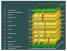
Define layer stack
If you are doing a high-speed/high-frequency design, you can use the built-in impedance analyzer to ensure impedance control in your board. The Impedance Curve tool uses Simberian’s integrated electromagnetic field solver to customize the trace geometry to achieve target impedance values.
Define impedance curves for routing in high-speed PCB designs
Step 5: Define design rules and DFM requirements
The number of PCB design rule categories is large, and you may not need to use all of these available rules for every design. You can select/deselect individual rules by right-clicking on the rule in question from the list in the PCB Rules and Constraints Editor below.
PCB Rules and Constraints Editor in Altium Designer
The rules you do use, especially for manufacturing, should be within the specifications and tolerances of the PCB manufacturer’s equipment. Advanced designs such as impedance controlled designs and many high speed/high frequency designs may require very specific design rules to be followed to ensure your product works properly. Always check your component datasheet for these design rules. If necessary, you can create new design rules by following the steps of Altium Designer’s Design Rules Wizard.
Edit PCB Design Rules Wizard in Altium Designer
Altium Designer will treat your custom design rules like built-in design rules. As you place components, vias, drill holes, and traces, the unified design engine in Altium Designer automatically checks your layout against these rules and visually flags you if violations occur.
Step 6: Place components
Altium Designer offers a lot of flexibility and allows you to quickly place components on the board. You can arrange components automatically or place them manually. You can also use these options together, allowing you to take advantage of the speed of automatic placement and ensure your board is laid out according to good component placement guidelines. An additional advanced feature of the latest version of Altium Designer is the ability to arrange components into groups. You can define these groups in the PCB layout or on the schematic using Cross Selection Mode, which is accessible from the Tools menu.
Place components using cross selection mode
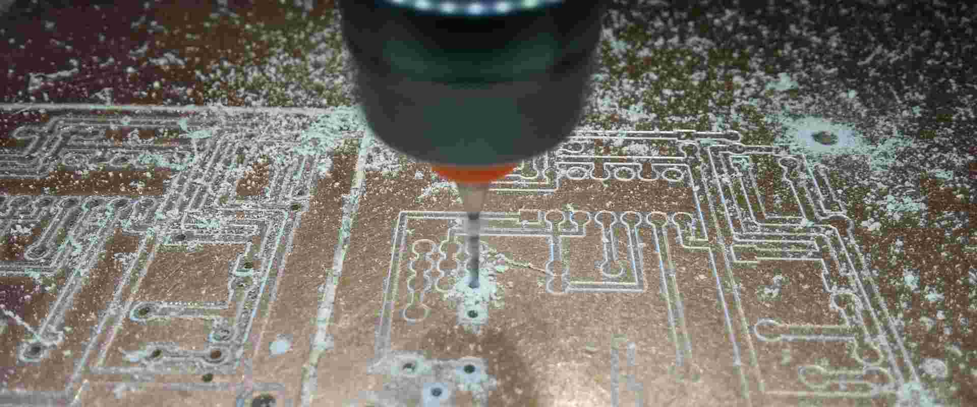
Step 7: Insert Drilled Holes
It’s a good idea to place drill holes (mounting and vias) before routing them. If your design is complex, you may need to modify at least some of the via locations during trace routing. This can be easily done through the Properties dialog box shown below.
Drill Options Dialog Box
Your preference here should follow the PCB manufacturer’s Design for Manufacturing (DFM) specifications. If you have defined your PCB DFM requirements as design rules (see step 5), Altium Designer will automatically check these rules when you place vias, drill holes, pads, and traces in your layout.
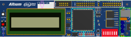
Step 8: Traceroute
Once the components and any other mechanical elements are placed, it’s time to prepare the wiring. Make sure to use good routing guidelines and take advantage of Altium Designer tools to simplify the process, such as net highlighting and color coding through routing, as shown below.
Color coding by routing
Altium Designer includes many important tools to help you simplify your wiring experience and increase your productivity. You’ll have access to a powerful autorouter and automated interactive routing tools. These tools will run on multiple networks simultaneously, making it easy to run large numbers of wires in series.
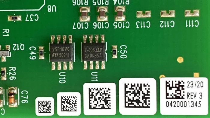
Step 9: Add tags and identifiers
Once your board layout is verified, you can add labels, identifiers, tags, logos, or any other images to your board. It is a good idea to use reference identifiers for components as this will aid in PCB assembly. Also include polarity indicators, pin 1 indicators, and any other labels that will help identify the component and its orientation. For logos and images, it’s best to check with your PCB manufacturer to make sure you’re using a readable font.
Label added to screen printing
Step 10: Generate Design Files
Before creating manufacturer deliverables, it is always best to verify the board layout by running a Design Rule Check (DRC). Altium Designer does this automatically as you lay out components and route your design, but it doesn’t hurt to run another DRC manually. If the board checks out, then you’re ready to release the manufacturer’s deliverables.
After the board passes the final DRC, you need to generate design files for the manufacturer. The design file should include all information and data needed to build the board; include any comments or special requirements to ensure your manufacturer is clear about your requirements. For most manufacturers, you will be able to use the Gerber file set shown below; however, some manufacturers prefer other CAD file formats.
GET PCB AND ASSEMBLY SERVICE QUOTE NOW!
A set of Gerber files
By following the steps above, the process of creating a comprehensive design is as easy as counting to ten. Using a systematic approach like this ensures that all aspects of the design are considered intrinsically during the design process without having to minimally retrace your steps.
Altium Designer is an advanced PCB design and development package that provides you with many tools to simplify otherwise difficult design tasks. However, the features and functionality discussed here only provide what is available to you from scratch. To explore these and other options, test the program yourself with the free trial. For more information about designing circuit boards with Altium Designer, contact an Altium Designer PCB design expert. You can also continue learning by listening to the Altium Podcast.