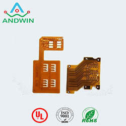
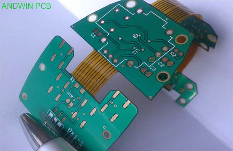
2 layer flex pcb stackup
The top layer is typically a copper layer that serves as the signal layer,
while the bottom layer is usually a ground plane or power plane.
The adhesive layer provides insulation and bonding between the two layers.

The thickness of the flexible material and the adhesive layer can vary depending on the specific requirements of the application.
The thickness of the copper layer is typically around 1 oz, or 35 microns.
In addition to the two layers, a coverlay or solder mask layer may be added to protect the copper traces and provide insulation.
A stiffener may also be added to provide support and stability to the flexible PCB.
Overall, a 2-layer flex PCB stackup provides a compact and flexible solution for applications where space is limited and flexibility is required.

here is the 2 layer flex pcb stackup used?
A 2-layer flex PCB stackup is commonly used in applications that require flexibility and compactness,
such as in wearable devices, medical devices, automotive electronics, and aerospace applications.