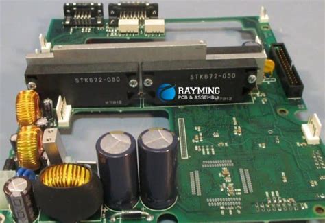
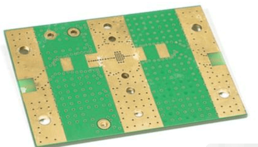
2 layer pcb ground plane
PCB grounding method:
There are many ways to connect the ground wires of each circuit to the ground plane, including:
Single-point and multi-point grounding methods
① Single-point grounding: The ground wires of all circuits are connected to the same point of the ground plane, which is divided into series single-point grounding and parallel single-point grounding.
② Multi-point grounding: The ground wires of all circuits are grounded nearby, and the ground wires are very short and suitable for high-frequency grounding.
③ Mixed grounding: Mix single-point grounding and multi-point grounding.
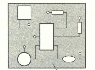
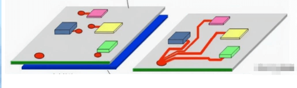
Single-point grounding is the most suitable for low frequency, low power and the same power layer, and is usually used in analog circuits; here, a star connection is generally used to reduce the influence of possible series impedance, as shown in the right half of Figure . High-frequency digital circuits need to be grounded in parallel, and here it can be handled more simply by using ground holes, as shown in the left half of the figure; generally, all modules will use a combination of two grounding methods, and use a mixed grounding method to complete the connection between the circuit ground wire and the ground plane.
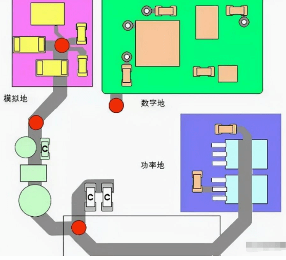
Mixed grounding method
If you do not choose to use the entire plane as a common ground line, for example, when the module itself has two ground lines, you need to split the ground plane, which often interacts with the power plane. Pay attention to the following principles:
(1) Align each plane to avoid overlap between irrelevant power planes and ground planes, otherwise all ground plane divisions will fail and interfere with each other;
(2) In the case of high frequency, the layers will be coupled through the parasitic capacitance of the circuit board;
(3) The signal lines between ground planes (such as digital ground planes and analog ground planes) are connected using ground bridges, and the nearest return path is configured through the nearest through-hole.
(4) Avoid running high-frequency lines such as clock lines near isolated ground planes to cause unnecessary radiation.
(5) The loop area formed by the signal line and its loop should be as small as possible, also known as the loop minimum rule; the smaller the loop area, the less external radiation and the less external interference. When splitting the ground plane and routing the signal, the distribution of the ground plane and important signal lines should be considered to prevent problems caused by ground plane slots, etc.
Here are some methods for connecting grounds.
① Ordinary wiring connection between ground circuit boards: This method can ensure reliable low-impedance conduction between the two ground wires, but it is limited to the connection between the grounds of medium and low-frequency signal circuits.
② Large resistance connection between grounds: The characteristic of large resistance is that once a voltage difference appears across the resistor, a very weak conduction current will be generated. After the charge on the ground wire is discharged, the voltage difference between the two ends will eventually be zero.
③ Capacitor connection between grounds: The characteristics of capacitors are DC cutoff and AC conduction, and they are used in floating ground systems.
④ Magnetic bead connection between grounds: Magnetic beads are equivalent to a resistor that changes with frequency, and they show resistance characteristics. It is used between grounds of weak signals with fast and small current fluctuations.
⑤ Inductor connection between grounds: Inductors have the characteristics of suppressing changes in circuit states, and can cut peaks and fill valleys. They are usually used between two grounds with large current fluctuations.
⑥ Small resistor connection between ground and earth: The small resistor adds a damping to hinder the overshoot of rapid changes in ground current; when the current changes, the rising edge of the impact current slows down.
Using a 2-layer PCB ground plane is also preferable to routing ground traces alone. Routing return traces adjacent to signal traces is one strategy for minimizing EMI susceptibility in multi-board designs when high-speed/high-frequency signals are routed between boards via cables. Placing the ground return as close as possible to the signal line allows the return signal to follow the trace closely, minimizing loop inductance and EMI susceptibility.
Almost every board with multiple components does not have enough room to route return traces next to all signal traces. Placing a ground plane on the bottom layer of a two-layer PCB provides the same effect; placing the ground plane underneath the signal traces also reduces the loop area seen by the signal. Ideally, signal traces should be as close to the ground plane as possible to suppress crosstalk between adjacent traces, which may require the use of a thinner board.
Placing a ground plane underneath the associated components and signal traces also allows you to route ground return paths directly from the components to the ground plane through vias. The return signal will then follow the path of least impedance back to the power supply return. This also allows you to easily place bypass/decoupling capacitors between the power connections and ground planes of critical components, allowing any high frequency fluctuations in the power connections (e.g. conducted EMI from switching power supplies) to reach the relevant components.
Preventing EMI with Proper Routing and Grounding Techniques
Ground Plane Screenshot Gridding
One technique that can be used in a two-layer PCB is gridding, rather than placing one continuous ground plane across the entire bottom layer. The power and ground traces are routed in a differential fashion, emulating a pair of power lines. Each ground trace can be extended to fill as much of the empty PCB space as possible, and all remaining empty space can be filled with ground fill. This technique will give your 2-layer board the same level of noise reduction as a four-layer PBC stackup.
Another solution is to use two perpendicular grid patterns on both layers, with the grids being connected with vias at the points where the grids cross. This ensures that all parts of the grid remain at nearly the same potential and provides some extra space for components on both layers. One potential issue with this design is routing between the single-layer grids. In this case, the ground trace can be routed next to the signal trace, where the ground trace is connected to the ground portion on the opposite layer through a via.
Like many design choices, gridding represents a trade-off: you gain more space on the board and can create low-inductance current loops through creative routing, but you lose some of the EMI protection provided by a continuous ground plane. The vias required for gridding also act as inductive impedance discontinuities, causing signal integrity issues for high-speed signals. Grids can also create conductive loops around components where radiated EMI can induce currents. A better option is to place components on one layer above another layer of ground grid.
In summary, be careful with grids. Some design guides will recommend using a grid in a two-layer board as an alternative to using a continuous ground plane on a single layer. This may be fine for low-speed/low-frequency signals or for DC boards with adequate shielding from the chassis. However, in high-speed/high-frequency situations without shielding or in environments with significant radiated EMI, it may be a better idea to sacrifice board space and choose a continuous ground plane on the bottom layer.
Mixed Signals—Creating Cross Sections in the Ground Plane
One technique that can be used in a two-layer PCB is to grid, rather than placing a continuous ground plane across the entire bottom layer. Power and ground traces are routed in a differential fashion, emulating a pair of power lines. Each ground trace can be extended to fill as much of the empty PCB space as possible, and all remaining empty space can be filled with ground fill. This technique will give your 2-layer board the same level of noise reduction as a four-layer PBC stackup.
Another solution is to use two perpendicular grid patterns on both layers, with the grids connected with vias at the points where the grids cross. This ensures that all parts of the grid remain at nearly the same potential and provides some extra space for components on both layers. One potential issue with this design is routing between grids on a single layer. In this case, a ground trace can be routed next to a signal trace, where the ground trace is connected to a ground section on the opposite layer by a via.
As with many design choices, gridding represents a trade-off: you gain more space on the board and can create low-inductance current loops with creative routing, but you lose some of the EMI protection provided by a continuous ground plane. The vias required for gridding also act as inductive impedance discontinuities, causing signal integrity issues for high-speed signals. Grids can also form conductive loops around components where radiated EMI can induce currents. A better option is to place components on one layer above another layer of ground grid.
In summary, be careful with grids. Some design guides will recommend using a grid in a two-layer board as an alternative to using a continuous ground plane on a single layer. This may be fine for low-speed/low-frequency signals or for DC boards with adequate shielding from the chassis. However, in high-speed/high-frequency situations without shielding or in environments with significant radiated EMI, it may be a better idea to sacrifice board space and opt for a continuous ground plane on the bottom layer.