2 layer pcb prototype
What are two layer pcbs
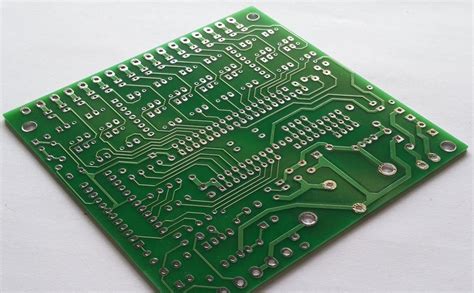
A 2 layer PCB is a printed circuit board with two layers of conductive copper traces.
These layers are known as the top and bottom layers.
It is also known as a double-sided PCB, which allows for a higher component density than single-sided PCBs.
You will find 2 layer PCBs used in a variety of electronic circuit applications in the electronics industry.
2 layer PCBs can be used for simple circuits as well as complex circuit structures.
Some common circuits that use 2 layer printed circuit boards include circuits for automotive applications, cellular devices, and equipment for testing, monitoring, and instrumentation.
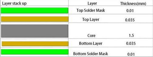
How are 2-layer PCBs constructed?
You will find 2-layer PCBs made by a lamination process where two copper foils are used to sandwich the substrate.
Fiberglass is often used as a substrate for printed circuit board construction.
How are components attached to 2-layer PCBs?
You will find two methods commonly used to attach components to 2-layer PCBs, through-hole mounting and surface mounting.
In through-hole connections, the leads of the components are inserted into drilled holes to secure them to the board.
Surface mount components are soldered to the surface of the board.
Surface mount offers the following benefits:
- SMT allows for compact arrangement of components, allowing for smaller boards in micro devices.
- You find that SMT does not require holes, thus reducing drilling costs.
- The component attaching process for surface mount is faster than through-hole mounting.
- 2-layer boards with SMT are very compact, allowing for faster performance.
- You find that surface mount components can be accommodated on both the top and bottom layers, allowing for increased density.
- SMT reduces induction, eliminating the adverse effects of RF interference.
However, you find that SMT is limited in the following ways:
- The tight fit of surface mount components makes repairing a difficult process. Additionally, soldering provides permanent joints that discourage replacement.
- The thermal cycling process used in the soldering process can damage the connection.
- SMT cannot be used for components that dissipate a lot of heat, as they can damage the solder joints through melting.
- You find that surface mount components are susceptible to rough handling and physical stress conditions.
On the other hand, you find the following benefits of through-hole mounting:
- Through-hole mounting is reliable because it provides a more secure board connection for components.
- You will find that through-hole mounted components can withstand greater stress conditions without breaking the board connection.
However, setbacks associated with through-hole mounting include:
- Drilling the holes required for through-hole mounting increases overall board cost and time.
- Tracking is limited in through-hole board configurations, especially when there are multiple layers.
- It takes longer to place components on a board using through-hole mounting than SMT.
- The soldering technique for through-hole mounting requires a double-sided operation and does not support repeatability
Can a board be 2-layer and have components on only one side?
Yes, it can.
A board can be 2-layer and have components on only one side of the board if the conductive traces are on the other side.
What makes a printed circuit board a 2-layer PCB is not the presence of components on both sides of the board.
Rather, it is the presence of conductive traces originating from one layer of copper foil.
Are arrays used to manufacture 2-layer PCBs?
Yes, they are.
Arrays can be used to manufacture 2-layer PCBs for large-scale orders, allowing for automation and repeatability.
There are two common alternatives to arrays that can be used alone or in combination: scoring and tab routing.
The combination of arrays serves complex designs with undefined margins.
Scoring in arrays is used for 2-layer board designs with uniform edges.
The feature of this technique is reduced material waste, which saves material costs.
Panel layers are stacked on top of each other for scoring.
You will find the material savings more pronounced for large productions.
Tab routing is suitable for 2-layer board designs with non-standardized shapes.
Additionally, you can use a tab routing array when you want to place components along the periphery of the board.
In this array, a margin of less than a quarter inch is provided between the boards.
Tab routing is supported using rails to aid assembly.
What material is used for the base of a 2-layer PCB?
Non-conductive material is used for 2-layer PCB substrates.
It is called a base material and is usually made of fiberglass reinforced with epoxy resin.
You can change the substrate material to make your board flexible or rigid.
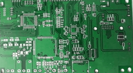
Do 2-layer PCBs use solder mask?
Yes.
The solder mask provides protection to the copper paths of both layers from oxidation during the soldering process.
Also, since solder is conductive, it can create an undesirable conductive path when allowed to interact with the copper traces.
Some of the materials used to create solder mask include epoxy liquid, which is the cheapest, and is formed by screen printing.
Liquid imageable inks are applied by screen printing or spraying.
Dry film photoimageable solder mask applied by a vacuum lamination process.
How do you solder 2-layer PCBs
Unlike single-sided boards, where the soldering process may not be too complicated, soldering two-layer PCBs is challenging.
This is especially true when performed manually.
However, you can greatly simplify the soldering process of 2-layer PCBs by:
- Using a pick and place device
- Using a CNC milling machine
Soldering involves the use of flux and solder paste.
The role of flux is to clean the assembly and remove unwanted particles, such as rust.
Additionally, it reduces the chances of rust by locking out air during the soldering process while enhancing solder dripping.
Solder paste is used to attach components to the board.
What are the advantages of 2-layer PCBs?
You will find that 2-layer PCBs have the following attractive features that make them the first choice for many PCB designs:
- You can achieve higher component density with 2-layer PCBs
- 2-layer PCBs allow copper traces to be routed closer than single-sided PCBs.
- 2-layer PCBs can find simplified and diverse uses in different circuit needs.
- 2-layer PCBs are cheaper compared to other multi-layer printed circuit boards.
- You will find that 2-layer PCBs have higher circuit density compared to single-sided boards.
- With 2-layer PCBs, you can make smaller boards with a higher number of components than single-sided boards.
- The configuration of 2-layer boards allows for a variety of uses, such as using the bottom layer as a copper pour or ground plane.
- You can also use 2-layer PCBs as current sources in electrical systems.
- Components can be better managed with 2-layer PCBs because they can be organized on both surfaces. You can use through-hole components on the top layer and surface mount components on the bottom layer.
- 2-layer PCBs can be used to accommodate ground and common collector voltages through the bottom layer. Using this approach allows the size of the board to remain the same.
Are vias used in 2-layer PCBs?
A through-hole has a drilled hole plated with a conductive material to allow electrical transfer between multiple layers.
There are three types of vias: blind, through-hole, and buried.
Blind and buried vias are associated with the inner layers that are missing in 2-layer PCBs.
Therefore, only through-holes are used in 2-layer PCBs.
Vias provide electrical connections between the top and bottom layers.
What copper weight is used in 2-layer PCBs?
The weight of copper in a PCB is measured in ounces (oz) over a square foot.
The copper weight helps determine the thickness of the conductive traces.
Also, the layers of a 2-layer PCB typically use half-ounce, single-ounce, or 2-ounce copper weights.
You will find a 1-ounce copper PCB in two-layer form with half-ounce weights per layer.
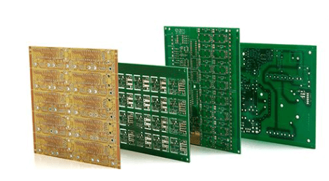
1-ounce copper PCB
Likewise, a 2 ounce copper PCB will have two layers, each containing 2 ounces of copper.
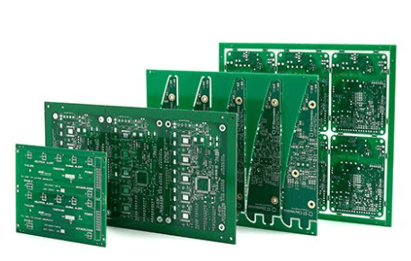
2 ounce copper PCB
Can a 2 oz copper PCB be formed with a 4 layer PCB?
Yes.
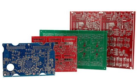
A 4 oz copper PCB can be made into a 2 layer PCB configuration.
4 oz copper PCB
You find that this can be achieved by using layers each made of 2 ounce copper.
The structure is such that a core of the substrate is made and laminated with two 2 ounce copper films.
What holes are drilled on 2 layer PCBs?
There are two types of holes drilled on 2 layer PCBs.
You will find plated holes and non-plated holes.
Plated holes are close to the edge of the board.
They are lined with conductive material, such as copper, to enable heat and electrical transfer.
Non-plated holes are plain wall holes that have no conductive capabilities.
These holes are usually spaced no less than half a millimeter apart and have a hole diameter of 0.5 mm.
To drill the holes, a CNC machine with a drill is used.
The entire arrangement and pattern depends on the PCB design.
The plating of the holes extends outside the hole, forming a flat bottom at the entry and exit points.
How are traces determined on 2 layer PCBs?
Traces on 2 layer PCBs serve as conductive paths for charge transfer.
The conductive trace parameters of trace width and trace spacing are determined by the copper weight of that layer.
In addition, you will find current requirements and component density useful in establishing trace parameters.
What is impedance control about 2 layer PCBs?
Impedance refers to the sum of reactance, resistance, and conductance exhibited by a circuit in a 2-layer PCB.
Impedance control aims to minimize the effects of impedance during board operation.
Furthermore, impedance is affected by the conductive path length and dielectric properties of the core.
In addition, impedance values can affect the operation of 2-layer PCBs used in high-power and high-speed applications.
Impedance effects are evidenced by increases in signal deflection and distortion.
If left unchecked, impedance can compromise RF transmissions.
Impedance control minimizes signal deflection while mitigating signal distortion by considering impedance values during the design phase.
You can identify materials with properties that are less susceptible to impedance erosion.
Additionally, because the potential for impedance increases with the number of layers, layer arrangement needs to be considered.
What routing methods can be used for 2-layer PCBs?
Routing adds wires on the PCB to enable proper component connections.
Single-board projects can be routed individually for individual boards.
For multi-boards, palletizing and V-score routing can be performed.
These boards are arranged in arrays, more commonly seen in automated assembly processes.
How is Silk Screen Applied on 2 Layer PCBs?
Silk Screen is a sheet of information placed on the solder mask.
It provides information related to the board and the components used by using features and symbols.
Some of this information includes test points, part numbers, manufacturer information, and component identifiers.
You can find two common methods of applying silk screen to 2 layer PCBs.
Silk screen can be applied through screen printing, where the required information is printed on a stencil.
Inkjet printers can also be used to print silk screen by digitizing the information.
Why are tolerances important in 2 layer PCBs?
2 Layer Printed Circuit Boards
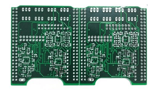
Tolerances are the allowances for dimensions such as hole and pad sizes associated with 2 layer PCBs.
Tolerances are useful because it provides flexibility to your design while adhering to the spirit of design for manufacturability.
What finishes are used for 2 layer PCBs?
2 layer PCBs are available in a variety of finishes.
Some common finishes include:
- Immersion silver, which provides a smooth surface while offering good solderability. However, you will find that this finish is limited in its ability to handle environmental factors such as temperature and humidity.
- Hot air solder levels with longer shelf life and secure solder joints. A smooth finish is difficult to achieve with this finish type, making it less suitable for fine finish requirements.
- Electroless nickel/immersion gold is favored for its smooth surface, secure solder joints, and resistance to environmental factors such as temperature and humidity. ENIG is also very flexible in finding uses for different designs.
What are Gold Fingers on 2-layer PCBs?
Gold Fingers PCB
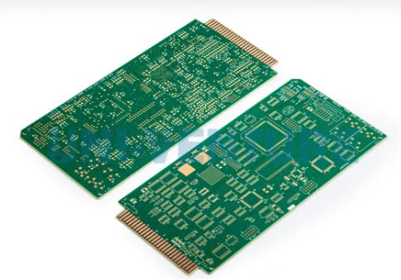
Gold Fingers are used to indicate edge terminations of connectors used to plug into 2-layer PCBs.
Gold fingers are made of hardened gold, providing a smooth surface and high wear resistance even with frequent use.
Gold fingers can be used with other types of surface treatments to enhance solderability and prevent wear.
What quality testing methods are used for 2-layer PCBs?
Testing of 2-layer PCBs helps determine if the 2-layer PCB meets the design requirements.
It also evaluates its reliability across two-layer structures.
Electrical testing can be performed on a 2-layer PCB without components and when it is populated.
You will find electrical testing helpful in establishing shorts and opens on the top and bottom layers of the PCB.
In this test, flying probes are used to identify electrical isolation points and unwanted connections.
Before component assembly on the board, the faults are corrected and tested again.
Identifying faults before assembly can minimize board failures.
If ignored, the cost of handling errors especially after populating the board can be significant.
2-layer PCBs can also be tested when components have been connected to find faults related to the assembly process.
With this test, you can determine functional failures of the board and connected components.
What are the quality standards for 2-layer PCBs?
The following include some of the standards provided for 2-layer PCBs:
· BS-123200-003
This standard provides quality assessment of rigid 2-layer PCBs with plated through holes.
· BS-EN-61249-2-2
In this standard, materials used for 2-layer PCBs and their interconnect structures are provided.
· BS-CECC-23100-801
This standard is a uniform system for assessing the quality of electronic components used on 2-layer PCBs with non-plated holes.
· BS-6221-4
This standard provides a specification method for 2-layer PCBs with non-plated holes.
· BS-IEC-61189-5-3
This standard provides common test procedures for electrical materials and interconnects on 2-layer PCBs.
It also provides guidelines for using solder paste on PCBs.
·DD-IEC/PAS-62326-7-1
This standard specifically addresses the performance of single-layer and 2-layer PCBs.
As you can see, there are many factors that should be considered when purchasing a 2-layer PCB.


